参数资料
| 型号: | PS8551L4-V-AX |
| 厂商: | CEL |
| 文件页数: | 14/18页 |
| 文件大小: | 0K |
| 描述: | ISOLATOR AMP ANALOG 5KRMS 8SMD |
| 标准包装: | 50 |
| 放大器类型: | 隔离 |
| 电路数: | 1 |
| 输出类型: | 差分 |
| -3db带宽: | 100kHz |
| 电流 - 输入偏压: | 500nA |
| 电压 - 输入偏移: | 300µV |
| 电流 - 电源: | 16mA |
| 电流 - 输出 / 通道: | 18.6mA |
| 电压 - 电源,单路/双路(±): | 4.5 V ~ 5.5 V |
| 工作温度: | -40°C ~ 85°C |
| 安装类型: | 表面贴装 |
| 封装/外壳: | 8-SMD |
| 供应商设备封装: | 8-DIP 鸥翼型 |
| 包装: | 散装 |
PS8551L4
Chapter Title
7
1
f
o
5
e
g
a
P
0
.
2
.
v
e
R
0
2
0
J
E
9
3
0
S
D
8
0
R
Sep 06, 2011
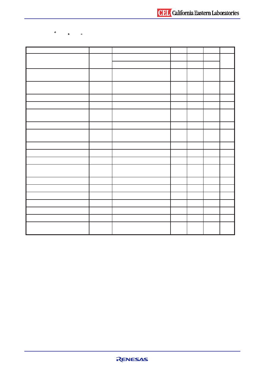
ELECTRICAL CHARACTERISTICS (DC Characteristics)
(TYP.: TA = 25°C, VIN+ = VIN = 0 V, VDD1 = VDD2 = 5 V,
MIN., MAX.: refer to RECOMMENDED OPERATING CONDITIONS, unless otherwise specified)
Parameter
Symbol
Conditions
MIN.
TYP.
MAX.
Unit
V
e
g
a
tl
o
V
t
e
sf
f
O
t
u
p
n
I
os
TA = 25°C
2
0.3
2
mV
3
Input Offset Voltage Drift
vs. Temperature
dVos/dTA TA = 25 to +85°C
3
10
μ
V/°C
Gain*1
G
200 mV ≤ VIN+ ≤ 200 mV,
TA = 25°C
7.76
8
8.24
V/V
Gain Drift vs. Temperature
dG/dTA
V
/
V
7
8
0
.
0
°
C
VOUT Non-linearity (200 mV)*2
NL200
200 mV ≤ VIN+ ≤ 200 mV
0.021
0.35
%
VOUT Non-linearity (200 mV) Drift
vs. Temperature
dNL200/dTA
/
%
2
0
.
0
°
C
VOUT Non-linearity (100 mV)*2
NL100
100 mV ≤ VIN+ ≤ 100 mV
0.014
0.2
%
Maximum Input Voltage before VOUT
Clipping
VIN+
V
m
8
0
3
.
X
A
M
I
t
n
e
rr
u
C
yl
p
u
S
t
u
p
n
I
DD
1
VIN+
A
m
0
2
6
1
V
m
0
4
=
Output Supply Current
IDD2
VIN+ =
A
m
6
1
0
1
V
m
0
4
I
t
n
e
rr
u
C
s
ai
B
t
u
p
n
I
IN+
VIN+ V
0
=
0.5
5
μ
A
Input Bias Current Drift
vs. Temperature
dIIN+/dTA
/
A
n
5
4
.
0
°
C
Low Level Saturated Output Voltage
VOL
VIN+ =
V
9
2
.
1
V
m
0
4
High Level Saturated Output Voltage
VOH
VIN+
V
8
.
3
V
m
0
4
=
Output Voltage (VIN+ = VIN = 0 V)
VOCM
VIN+ = VIN
V
8
.
2
5
.
2
.
2
V
0
=
Output Short-circuit Current
IOSC
A
m
6
.
8
1
Equivalent Input Resistance
RIN
k
0
2
3
Ω
VOUT Output Resistance
ROUT
5
1
Ω
Input DC Common-Mode Rejection
Ratio*3
CMRRIN
B
d
6
7
*1 The differential output voltage (VOUT+ VOUT) with respect to the differential input voltage (VIN+ VIN), where VIN+ =
200 mV to 200 mV and VIN = 0 V) is measured under the circuit shown in Fig. 2 NL200, G Test Circuit. Upon
the resulting chart, the gain is defined as the slope of the optimum line obtained by using the method of least
squares.
*2 The differential output voltage (VOUT+ VOUT) with respect to the differential input voltage (VIN+ VIN) is measured
under the circuit shown in Fig. 2 NL200, G Test Circuit. Upon the resulting chart, the optimum line is obtained by
using the method of least squares. Non-linearity is defined as the ratio (%) of the optimum line obtained by dividing
[Half of the peak to peak value of the (residual) deviation] by [full-scale differential output voltage].
For example, if the differential output voltage is 3.2 V, and the peak to peak value of the (residual) deviation is 22.4
mV, while the input VIN+ is ±200 mV, the output non-linearity is obtained as follows:
NL200 = 22.4/(2 × 3 200) = 0.35%
*3 CMRRIN is defined as the ratio of the differential signal gain (when the differential signal is applied between the
input pins) to the common-mode signal gain (when both input pins are connected and the signal is applied). This
value is indicated in dB.
<R>
A Business Partner of Renesas Electronics Corporation.
相关PDF资料 |
PDF描述 |
|---|---|
| PSB2-1ND | HEATSINK V/H W/TABS NICKL TO-220 |
| PUM-3046L-R | MIC CONDENSER ELECT UNI -46+-3DB |
| PUM-3546L-R | MIC CONDENSER ELECT UNI -46+-3DB |
| PUM-5250L-R | MIC CONDENSER ELECT UNI -50DB |
| PW3 | WASHER COMPRESSION SNP SERIES |
相关代理商/技术参数 |
参数描述 |
|---|---|
| PS8551L4-V-E3 | 制造商:RENESAS 制造商全称:Renesas Technology Corp 功能描述:ANALOG OUTPUT TYPE OPTICAL COUPLED ISOLATION AMPLIFIER |
| PS86 | 制造商:未知厂家 制造商全称:未知厂家 功能描述:Analog IC |
| PS860 | 制造商:未知厂家 制造商全称:未知厂家 功能描述:Analog IC |
| PS8601 | 功能描述:高速光耦合器 Hi-Speed Analog Out RoHS:否 制造商:Avago Technologies 电流传递比: 最大波特率: 最大正向二极管电压:1.75 V 最大反向二极管电压:5 V 最大功率耗散:40 mW 最大工作温度:+125 C 最小工作温度:- 40 C 封装 / 箱体:SOIC-5 封装:Tube |
| PS8601-A | 功能描述:高速光耦合器 Hi-Speed Analog Out RoHS:否 制造商:Avago Technologies 电流传递比: 最大波特率: 最大正向二极管电压:1.75 V 最大反向二极管电压:5 V 最大功率耗散:40 mW 最大工作温度:+125 C 最小工作温度:- 40 C 封装 / 箱体:SOIC-5 封装:Tube |
发布紧急采购,3分钟左右您将得到回复。