- 您现在的位置:买卖IC网 > PDF目录368208 > PSD4235F1-C-90MI (意法半导体) Flash In-System-Programmable Peripherals for 16-Bit MCUs PDF资料下载
参数资料
| 型号: | PSD4235F1-C-90MI |
| 厂商: | 意法半导体 |
| 英文描述: | Flash In-System-Programmable Peripherals for 16-Bit MCUs |
| 中文描述: | Flash在系统可编程外设的16位微控制器 |
| 文件页数: | 13/93页 |
| 文件大小: | 503K |
| 代理商: | PSD4235F1-C-90MI |
第1页第2页第3页第4页第5页第6页第7页第8页第9页第10页第11页第12页当前第13页第14页第15页第16页第17页第18页第19页第20页第21页第22页第23页第24页第25页第26页第27页第28页第29页第30页第31页第32页第33页第34页第35页第36页第37页第38页第39页第40页第41页第42页第43页第44页第45页第46页第47页第48页第49页第50页第51页第52页第53页第54页第55页第56页第57页第58页第59页第60页第61页第62页第63页第64页第65页第66页第67页第68页第69页第70页第71页第72页第73页第74页第75页第76页第77页第78页第79页第80页第81页第82页第83页第84页第85页第86页第87页第88页第89页第90页第91页第92页第93页
PSD4000 Series
Preliminary Information
10
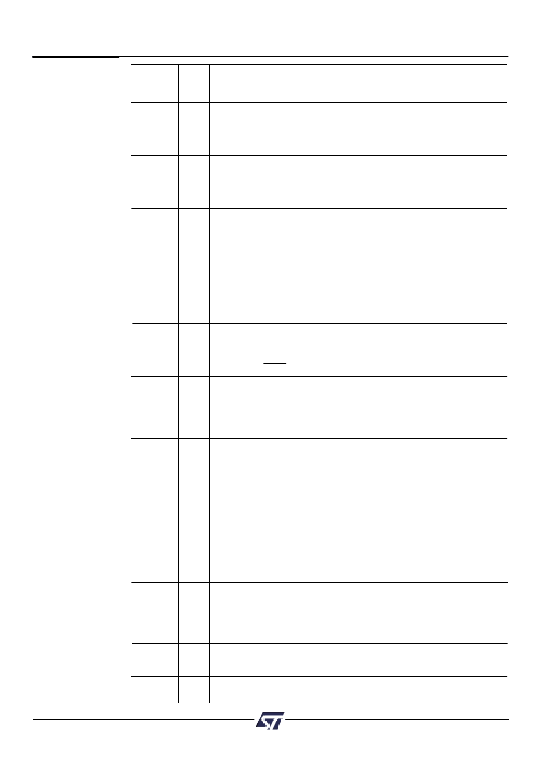
Pin*
(TQFP
Pin Name Pkg.)
Type
Description
PE1
72
I/O
Port E, PE1. This port is pin configurable and has multiple
functions:
1. MCU I/O — standard output or input port.
2. Latched address output.
3. TCK input for JTAG/ISP interface (Schmidt Trigger).
Port E, PE2. This port is pin configurable and has multiple
functions:
1. MCU I/O — standard output or input port.
2. Latched address output.
3. TDI input for JTAG/ISP interface.
Port E, PE3. This port is pin configurable and has multiple
functions:
1. MCU I/O — standard output or input port.
2. Latched address output.
3. TDO output for JTAG/ISP interface.
Port E, PE4. This port is pin configurable and has multiple
functions:
1. MCU I/O — standard output or input port.
2. Latched address output.
3. TSTAT output for the ISP interface.
4. Rdy/Bsy — for in-circuit Parallel Programming.
Port E, PE5. This port is pin configurable and has multiple
functions:
1. MCU I/O — standard output or input port.
2. Latched address output.
3. TERR active low output for ISP interface.
Port E, PE6. This port is pin configurable and has multiple
functions:
1. MCU I/O — standard output or input port.
2. Latched address output.
3. Vstby — SRAM standby voltage input for battery
backup SRAM
Port E, PE7. This port is pin configurable and has multiple
functions:
1. MCU I/O — standard output or input port.
2. Latched address output.
3. Vbaton — battery backup indicator output. Goes high when
power is drawn from an external battery.
Port F, PF0-7. This port is pin configurable and has multiple
functions:
1. MCU I/O — standard output or input port.
2. Input to the PLD.
3. Latched address outputs.
4. As address A1-3 inputs in 80C51XA mode (PF0 is grounded)
5. As data bus port (D0-7) in non-multiplexed bus configuration
6. MCU reset mode.
Port G, PG0-7. This port is pin configurable and has multiple
functions:
1. MCU I/O — standard output or input port.
2. Latched address outputs.
3. As data bus port (D8-15) in non-multiplexed bus configuration.
4. MCU reset mode.
CMOS
or Open
Drain
PE2
73
I/O
CMOS
or Open
Drain
PE3
74
I/O
CMOS
or Open
Drain
PE4
75
I/O
CMOS
or Open
Drain
PE5
76
I/O
CMOS
or Open
Drain
PE6
77
I/O
CMOS
or Open
Drain
PE7
78
I/O
CMOS
or Open
Drain
PF0-PF7
31-38
I/O
CMOS
or Open
Drain
PG0-PG7 21-28
I/O
CMOS
or Open
Drain
GND
8,30,
49,50,
70
9,29,
69
V
CC
Table 5.
PSD4000
Pin
Descriptions
(cont.)
相关PDF资料 |
PDF描述 |
|---|---|
| PSD4235F1-C-90U | Flash In-System-Programmable Peripherals for 16-Bit MCUs |
| PSD4235F1-C-90UI | Flash In-System-Programmable Peripherals for 16-Bit MCUs |
| PSD4235F2-15UI | Flash In-System-Programmable Peripherals for 16-Bit MCUs |
| PSD4235F2-70UI | Flash In-System-Programmable Peripherals for 16-Bit MCUs |
| PSD4235F2-90B81 | Flash In-System-Programmable Peripherals for 16-Bit MCUs |
相关代理商/技术参数 |
参数描述 |
|---|---|
| PSD4235G2-70U | 功能描述:SPLD - 简单可编程逻辑器件 5.0V 4M 70ns RoHS:否 制造商:Texas Instruments 逻辑系列:TICPAL22V10Z 大电池数量:10 最大工作频率:66 MHz 延迟时间:25 ns 工作电源电压:4.75 V to 5.25 V 电源电流:100 uA 最大工作温度:+ 75 C 最小工作温度:0 C 安装风格:Through Hole 封装 / 箱体:DIP-24 |
| PSD4235G2-90U | 功能描述:CPLD - 复杂可编程逻辑器件 5.0V 4M 90ns RoHS:否 制造商:Lattice 系列: 存储类型:EEPROM 大电池数量:128 最大工作频率:333 MHz 延迟时间:2.7 ns 可编程输入/输出端数量:64 工作电源电压:3.3 V 最大工作温度:+ 90 C 最小工作温度:0 C 封装 / 箱体:TQFP-100 |
| PSD4235G2-90UI | 功能描述:CPLD - 复杂可编程逻辑器件 5.0V 4M 90ns RoHS:否 制造商:Lattice 系列: 存储类型:EEPROM 大电池数量:128 最大工作频率:333 MHz 延迟时间:2.7 ns 可编程输入/输出端数量:64 工作电源电压:3.3 V 最大工作温度:+ 90 C 最小工作温度:0 C 封装 / 箱体:TQFP-100 |
| PSD4235G2V-12UI | 功能描述:CPLD - 复杂可编程逻辑器件 3.3V 4M 120ns RoHS:否 制造商:Lattice 系列: 存储类型:EEPROM 大电池数量:128 最大工作频率:333 MHz 延迟时间:2.7 ns 可编程输入/输出端数量:64 工作电源电压:3.3 V 最大工作温度:+ 90 C 最小工作温度:0 C 封装 / 箱体:TQFP-100 |
| PSD4235G2V-90U | 功能描述:CPLD - 复杂可编程逻辑器件 3.3V 4M 90ns RoHS:否 制造商:Lattice 系列: 存储类型:EEPROM 大电池数量:128 最大工作频率:333 MHz 延迟时间:2.7 ns 可编程输入/输出端数量:64 工作电源电压:3.3 V 最大工作温度:+ 90 C 最小工作温度:0 C 封装 / 箱体:TQFP-100 |
发布紧急采购,3分钟左右您将得到回复。