- 您现在的位置:买卖IC网 > PDF目录368208 > PSD4235F1-C-90MI (意法半导体) Flash In-System-Programmable Peripherals for 16-Bit MCUs PDF资料下载
参数资料
| 型号: | PSD4235F1-C-90MI |
| 厂商: | 意法半导体 |
| 英文描述: | Flash In-System-Programmable Peripherals for 16-Bit MCUs |
| 中文描述: | Flash在系统可编程外设的16位微控制器 |
| 文件页数: | 54/93页 |
| 文件大小: | 503K |
| 代理商: | PSD4235F1-C-90MI |
第1页第2页第3页第4页第5页第6页第7页第8页第9页第10页第11页第12页第13页第14页第15页第16页第17页第18页第19页第20页第21页第22页第23页第24页第25页第26页第27页第28页第29页第30页第31页第32页第33页第34页第35页第36页第37页第38页第39页第40页第41页第42页第43页第44页第45页第46页第47页第48页第49页第50页第51页第52页第53页当前第54页第55页第56页第57页第58页第59页第60页第61页第62页第63页第64页第65页第66页第67页第68页第69页第70页第71页第72页第73页第74页第75页第76页第77页第78页第79页第80页第81页第82页第83页第84页第85页第86页第87页第88页第89页第90页第91页第92页第93页
Preliminary Information
PSD4000 Series
Drive
Register
Bit 7
Bit 6
Bit 5
Bit 4
Bit 3
Bit 2
Bit 1
Bit 0
Port A
Open
Drain
Open
Drain
Open
Drain
Open
Drain
Open
Drain
Open
Drain
Open
Drain
Open
Drain
Port B
Open
Drain
Open
Drain
Open
Drain
Open
Drain
Open
Drain
Open
Drain
Open
Drain
Open
Drain
Port C
Slew
Rate
Slew
Rate
Slew
Rate
Slew
Rate
Slew
Rate
Slew
Rate
Slew
Rate
Slew
Rate
Port D
Open
Drain
Open
Drain
Open
Drain
Open
Drain
Port E
Open
Drain
Open
Drain
Open
Drain
Open
Drain
Open
Drain
Open
Drain
Open
Drain
Open
Drain
Port F
Slew
Rate
Slew
Rate
Slew
Rate
Slew
Rate
Slew
Rate
Slew
Rate
Slew
Rate
Slew
Rate
Port G
Open
Drain
Open
Drain
Open
Drain
Open
Drain
Open
Drain
Open
Drain
Open
Drain
Open
Drain
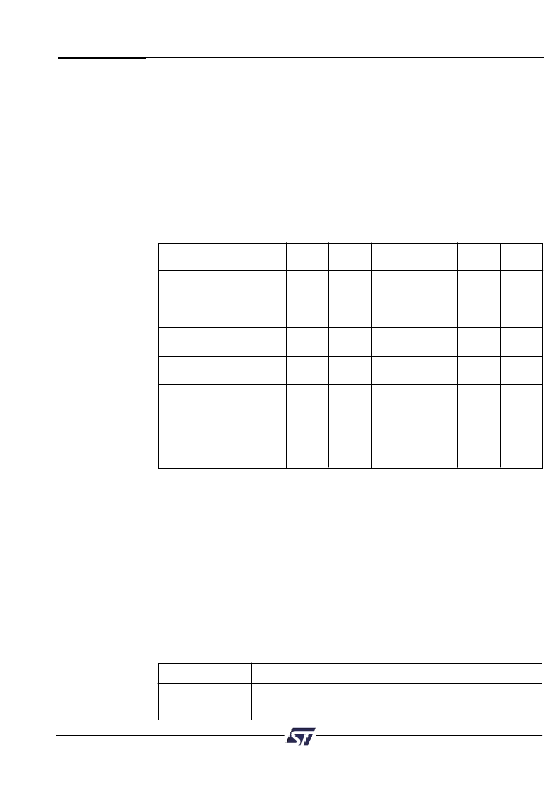
Table 22. Drive Register Pin Assignment
The
PSD4000
Functional
Blocks
(cont.)
9.4.3.3 Drive Select Register
The Drive Select Register configures the pin driver as Open Drain or CMOS for some port
pins, and controls the slew rate for the other port pins. An external pull-up resistor should
be used for pins configured as Open Drain.
A pin can be configured as Open Drain if its corresponding bit in the Drive Select Register
is set to a
‘
1
’
. The default pin drive is CMOS.
Aside:
the slew rate is a measurement of the rise and fall times of an output. A higher
slew rate means a faster output response and may create more electrical noise. A pin
operates in a high slew rate when the corresponding bit in the Drive Register is set to
‘
1
’
.
The default rate is slow slew.
Table 22 shows the Drive Register for Ports A, B, C, D, E, F and G. It summarizes which
pins can be configured as Open Drain outputs and which pins the slew rate can be set for.
51
9.4.4 Port Data Registers
The Port Data Registers, shown in Table 23, are used by the microcontroller to write data
to or read data from the ports. Table 23 shows the register name, the ports having each
register type, and microcontroller access for each register type. The registers are
described below.
9.4.4.1 Data In
Port pins are connected directly to the Data In buffer. In MCU I/O input mode, the pin input
is read through the Data In buffer.
9.4.4.2 Data Out Register
Stores output data written by the MCU in the MCU I/O output mode. The contents of the
Register are driven out to the pins if the Direction Register or the output enable
product term is set to
“
1
”
. The contents of the register can also be read back by the
microcontroller.
Table 27. Port Data Registers
Register Name
Port
MCU Access
Data In
A,B,C,D,E,F,G
Read
–
input on pin
Data Out
A,B,C,D,E,F,G
Write/Read
相关PDF资料 |
PDF描述 |
|---|---|
| PSD4235F1-C-90U | Flash In-System-Programmable Peripherals for 16-Bit MCUs |
| PSD4235F1-C-90UI | Flash In-System-Programmable Peripherals for 16-Bit MCUs |
| PSD4235F2-15UI | Flash In-System-Programmable Peripherals for 16-Bit MCUs |
| PSD4235F2-70UI | Flash In-System-Programmable Peripherals for 16-Bit MCUs |
| PSD4235F2-90B81 | Flash In-System-Programmable Peripherals for 16-Bit MCUs |
相关代理商/技术参数 |
参数描述 |
|---|---|
| PSD4235G2-70U | 功能描述:SPLD - 简单可编程逻辑器件 5.0V 4M 70ns RoHS:否 制造商:Texas Instruments 逻辑系列:TICPAL22V10Z 大电池数量:10 最大工作频率:66 MHz 延迟时间:25 ns 工作电源电压:4.75 V to 5.25 V 电源电流:100 uA 最大工作温度:+ 75 C 最小工作温度:0 C 安装风格:Through Hole 封装 / 箱体:DIP-24 |
| PSD4235G2-90U | 功能描述:CPLD - 复杂可编程逻辑器件 5.0V 4M 90ns RoHS:否 制造商:Lattice 系列: 存储类型:EEPROM 大电池数量:128 最大工作频率:333 MHz 延迟时间:2.7 ns 可编程输入/输出端数量:64 工作电源电压:3.3 V 最大工作温度:+ 90 C 最小工作温度:0 C 封装 / 箱体:TQFP-100 |
| PSD4235G2-90UI | 功能描述:CPLD - 复杂可编程逻辑器件 5.0V 4M 90ns RoHS:否 制造商:Lattice 系列: 存储类型:EEPROM 大电池数量:128 最大工作频率:333 MHz 延迟时间:2.7 ns 可编程输入/输出端数量:64 工作电源电压:3.3 V 最大工作温度:+ 90 C 最小工作温度:0 C 封装 / 箱体:TQFP-100 |
| PSD4235G2V-12UI | 功能描述:CPLD - 复杂可编程逻辑器件 3.3V 4M 120ns RoHS:否 制造商:Lattice 系列: 存储类型:EEPROM 大电池数量:128 最大工作频率:333 MHz 延迟时间:2.7 ns 可编程输入/输出端数量:64 工作电源电压:3.3 V 最大工作温度:+ 90 C 最小工作温度:0 C 封装 / 箱体:TQFP-100 |
| PSD4235G2V-90U | 功能描述:CPLD - 复杂可编程逻辑器件 3.3V 4M 90ns RoHS:否 制造商:Lattice 系列: 存储类型:EEPROM 大电池数量:128 最大工作频率:333 MHz 延迟时间:2.7 ns 可编程输入/输出端数量:64 工作电源电压:3.3 V 最大工作温度:+ 90 C 最小工作温度:0 C 封装 / 箱体:TQFP-100 |
发布紧急采购,3分钟左右您将得到回复。