- 您现在的位置:买卖IC网 > PDF目录376275 > PSD834F4V-70 (意法半导体) Flash In-System Programmable (ISP) Peripherals for 8-bit MCUs, 5V PDF资料下载
参数资料
| 型号: | PSD834F4V-70 |
| 厂商: | 意法半导体 |
| 英文描述: | Flash In-System Programmable (ISP) Peripherals for 8-bit MCUs, 5V |
| 中文描述: | Flash在系统可编程(ISP)的周边8位MCU,5V的 |
| 文件页数: | 92/110页 |
| 文件大小: | 1737K |
| 代理商: | PSD834F4V-70 |
第1页第2页第3页第4页第5页第6页第7页第8页第9页第10页第11页第12页第13页第14页第15页第16页第17页第18页第19页第20页第21页第22页第23页第24页第25页第26页第27页第28页第29页第30页第31页第32页第33页第34页第35页第36页第37页第38页第39页第40页第41页第42页第43页第44页第45页第46页第47页第48页第49页第50页第51页第52页第53页第54页第55页第56页第57页第58页第59页第60页第61页第62页第63页第64页第65页第66页第67页第68页第69页第70页第71页第72页第73页第74页第75页第76页第77页第78页第79页第80页第81页第82页第83页第84页第85页第86页第87页第88页第89页第90页第91页当前第92页第93页第94页第95页第96页第97页第98页第99页第100页第101页第102页第103页第104页第105页第106页第107页第108页第109页第110页
PSD813F2, PSD833F2, PSD834F2, PSD853F2, PSD854F2
92/110
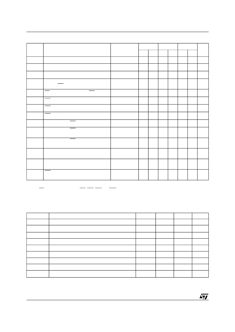
Table 58. WRITE Timing (3V devices)
Note: 1. Any input used to select an internal PSD function.
2. In multiplexed mode, latched address generated from ADIO delay to address output on any port.
3. WR has the same timing as E, LDS, UDS, WRL, and WRH signals.
4. Assuming data is stable before active WRITE signal.
5. Assuming WRITE is active before data becomes valid.
6. TWHAX2 is the address hold time for DPLD inputs that are used to generate Sector Select signals for internal PSD memory.
Table 59. Program, WRITE and Erase Times (5V devices)
Symbol
Note: 1. Programmed to all zero before erase.
2. The polling status, DQ7, is valid tQ7VQV time units before the data byte, DQ0-DQ7, is valid for reading.
Symbol
Parameter
Conditions
-12
-15
-20
Unit
Min
Max
Min
Max
Min
Max
t
LVLX
ALE or AS Pulse Width
26
26
30
t
AVLX
Address Setup Time
(Note
1
)
9
10
12
ns
t
LXAX
Address Hold Time
(Note
1
)
9
12
14
ns
t
AVWL
Address Valid to Leading
Edge of WR
(Notes
1,3
)
17
20
25
ns
t
SLWL
CS Valid to Leading Edge of WR
(Note
3
)
17
20
25
ns
t
DVWH
WR Data Setup Time
(Note
3
)
45
45
50
ns
t
WHDX
WR Data Hold Time
(Note
3
)
7
8
10
ns
t
WLWH
WR Pulse Width
(Note
3
)
46
48
53
ns
t
WHAX1
Trailing Edge of WR to Address Invalid
(Note
3
)
10
12
17
ns
t
WHAX2
Trailing Edge of WR to DPLD Address
Invalid
(Note
3,6
)
0
0
0
ns
t
WHPV
Trailing Edge of WR to Port Output
Valid Using I/O Port Data Register
(Note
3
)
33
35
40
ns
t
DVMV
Data Valid to Port Output Valid
Using Macrocell Register Preset/Clear
(Notes
3,5
)
70
70
80
ns
t
AVPV
Address Input Valid to Address
Output Delay
(Note
2
)
33
35
40
ns
t
WLMV
WR Valid to Port Output Valid Using
Macrocell Register Preset/Clear
(Notes
3,4
)
70
70
80
ns
Parameter
Min.
Typ.
Max.
Unit
Flash Program
8.5
s
Flash Bulk Erase
1
(pre-programmed)
3
30
s
Flash Bulk Erase (not pre-programmed)
5
s
t
WHQV3
Sector Erase (pre-programmed)
1
30
s
t
WHQV2
Sector Erase (not pre-programmed)
2.2
s
t
WHQV1
Byte Program
14
1200
μs
Program / Erase Cycles (per Sector)
100,000
cycles
t
WHWLO
Sector Erase Time-Out
100
μs
t
Q7VQV
DQ7 Valid to Output (DQ7-DQ0) Valid (Data Polling)
2
30
ns
相关PDF资料 |
PDF描述 |
|---|---|
| PSD854F4V-70 | Flash In-System Programmable (ISP) Peripherals for 8-bit MCUs, 5V |
| PSD814F4V-90 | Flash In-System Programmable (ISP) Peripherals for 8-bit MCUs, 5V |
| PSD834F5V-20 | Flash In-System Programmable (ISP) Peripherals for 8-bit MCUs, 5V |
| PSD854F5V-20 | Flash In-System Programmable (ISP) Peripherals for 8-bit MCUs, 5V |
| PSD814F5V-70 | Flash In-System Programmable (ISP) Peripherals for 8-bit MCUs, 5V |
相关代理商/技术参数 |
参数描述 |
|---|---|
| PSD835G2-70U | 功能描述:静态随机存取存储器 5.0V 4M 70ns RoHS:否 制造商:Cypress Semiconductor 存储容量:16 Mbit 组织:1 M x 16 访问时间:55 ns 电源电压-最大:3.6 V 电源电压-最小:2.2 V 最大工作电流:22 uA 最大工作温度:+ 85 C 最小工作温度:- 40 C 安装风格:SMD/SMT 封装 / 箱体:TSOP-48 封装:Tray |
| PSD835G2-90U | 功能描述:静态随机存取存储器 5.0V 4M 90ns RoHS:否 制造商:Cypress Semiconductor 存储容量:16 Mbit 组织:1 M x 16 访问时间:55 ns 电源电压-最大:3.6 V 电源电压-最小:2.2 V 最大工作电流:22 uA 最大工作温度:+ 85 C 最小工作温度:- 40 C 安装风格:SMD/SMT 封装 / 箱体:TSOP-48 封装:Tray |
| PSD835G2-90UI | 功能描述:静态随机存取存储器 5.0V 4M 90ns RoHS:否 制造商:Cypress Semiconductor 存储容量:16 Mbit 组织:1 M x 16 访问时间:55 ns 电源电压-最大:3.6 V 电源电压-最小:2.2 V 最大工作电流:22 uA 最大工作温度:+ 85 C 最小工作温度:- 40 C 安装风格:SMD/SMT 封装 / 箱体:TSOP-48 封装:Tray |
| PSD835G2V-12UI | 功能描述:静态随机存取存储器 3.0V 4M 120ns RoHS:否 制造商:Cypress Semiconductor 存储容量:16 Mbit 组织:1 M x 16 访问时间:55 ns 电源电压-最大:3.6 V 电源电压-最小:2.2 V 最大工作电流:22 uA 最大工作温度:+ 85 C 最小工作温度:- 40 C 安装风格:SMD/SMT 封装 / 箱体:TSOP-48 封装:Tray |
| PSD835G2V-90U | 功能描述:静态随机存取存储器 3.0V 4M 90ns RoHS:否 制造商:Cypress Semiconductor 存储容量:16 Mbit 组织:1 M x 16 访问时间:55 ns 电源电压-最大:3.6 V 电源电压-最小:2.2 V 最大工作电流:22 uA 最大工作温度:+ 85 C 最小工作温度:- 40 C 安装风格:SMD/SMT 封装 / 箱体:TSOP-48 封装:Tray |
发布紧急采购,3分钟左右您将得到回复。