- 您现在的位置:买卖IC网 > PDF目录368300 > PSD935G2V-C-90U (意法半导体) Configurable Memory System on a Chip for 8-Bit Microcontrollers PDF资料下载
参数资料
| 型号: | PSD935G2V-C-90U |
| 厂商: | 意法半导体 |
| 英文描述: | Configurable Memory System on a Chip for 8-Bit Microcontrollers |
| 中文描述: | 在8片位微控制器可配置存储系统 |
| 文件页数: | 17/91页 |
| 文件大小: | 488K |
| 代理商: | PSD935G2V-C-90U |
第1页第2页第3页第4页第5页第6页第7页第8页第9页第10页第11页第12页第13页第14页第15页第16页当前第17页第18页第19页第20页第21页第22页第23页第24页第25页第26页第27页第28页第29页第30页第31页第32页第33页第34页第35页第36页第37页第38页第39页第40页第41页第42页第43页第44页第45页第46页第47页第48页第49页第50页第51页第52页第53页第54页第55页第56页第57页第58页第59页第60页第61页第62页第63页第64页第65页第66页第67页第68页第69页第70页第71页第72页第73页第74页第75页第76页第77页第78页第79页第80页第81页第82页第83页第84页第85页第86页第87页第88页第89页第90页第91页
PSD9XX Family
PSD935G2
16
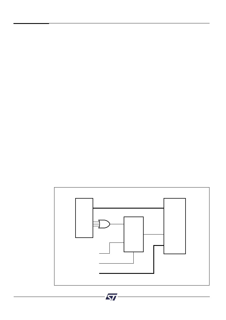
9.1.1.2 Upper and Lower Block IN MAIN FLASH SECTOR
The PSD935G2’s main Flash has eight 64K bytes sector. The 64K byte sector size may
cause some difficulty in code mapping for an 8-bit MCU with only 64K byte address space.
To resolve this mapping issue, the PSD935G2 provides additional logic (Figure 3) for the
user to split the 8 sectors such that each sector has a lower and upper 32K byte block, and
the two blocks can reside in different pages but in the same address range.
If your design works with 64KB sectors, you don’t need to configure this logic. If the design
requires 32KB blocks in each sector, you need to define a “FA15” PLD equation in
PSDsoft as the A15 address input to the main Flash module. FA15 consists of 3 product
terms and will control whether the MCU is accessing the lower or upper 32KB in the
selected sector. Below is an example for Flash sector chip select FS0. A typical equation
is FA15 = pgr4 of the Page Register. When pgr4 is 0 (page 00), the lower 32KB is
selected. When Pgr4 is switched to 1 by the user, the upper 32KB is selected. PSDsoft will
automatically generate the PLD equations shown, based on your point and click
selections.
page = [pgr7...pgr0]; “Page Register output
“Sector Chip Select Equation
FS0 = ((0000h <= address <= 7FFFh) & page = 00h) #
((0000h <= address <= 7FFFh) & page = 10h);
FA15 = pgr4;
“as address A15 input to the main Flash
“select first 32KB block
“select second 32KB block
If no FA15 equation is defined in PSDsoft, the A15 that comes from the MCU address bus
will be routed as input to the main Flash instead of FA15. The FA15 equation has no
impact in the Sector Erase operation. Note: FA15 affects all eight sectors of the main Flash
simultaneously, you cannot direct FA15 to a particular Flash sector only.
9.1.1.3 The Ready/Busy Pin (PE4)
Pin PE4 can be used to output the Ready/Busy status of the PSD935G2. The output on
the pin will be a ‘0’ (Busy) when Flash memory blocks are being written to,
or
when the
Flash memory block is being erased. The output will be a ‘1’ (Ready) when no write or
erase operation is in progress.
The
PSD935G2
Functional
Blocks
(cont.)
DPLD
ARRAY
FA15
A15
*
Set by PSDsoft
FLASH CHIP SELECTS FS0-7
MUX
NVM CONTROL BIT
*
MAIN
FLASH
SECTOR
ADDR A15
A [14:0]
Figure 3. Selecting the Upper or Lower Block in a Main Flash Sector
相关PDF资料 |
PDF描述 |
|---|---|
| PSD935G2V-C-90UI | Configurable Memory System on a Chip for 8-Bit Microcontrollers |
| PSD935G3-70U | Configurable Memory System on a Chip for 8-Bit Microcontrollers |
| PSD935G3-70UI | Configurable Memory System on a Chip for 8-Bit Microcontrollers |
| PSD935G3-90B81 | Configurable Memory System on a Chip for 8-Bit Microcontrollers |
| PSD935G3-90B81I | Configurable Memory System on a Chip for 8-Bit Microcontrollers |
相关代理商/技术参数 |
参数描述 |
|---|---|
| PSD954F2-90J | 功能描述:SPLD - 简单可编程逻辑器件 U 511-PSD854F2-90J RoHS:否 制造商:Texas Instruments 逻辑系列:TICPAL22V10Z 大电池数量:10 最大工作频率:66 MHz 延迟时间:25 ns 工作电源电压:4.75 V to 5.25 V 电源电流:100 uA 最大工作温度:+ 75 C 最小工作温度:0 C 安装风格:Through Hole 封装 / 箱体:DIP-24 |
| PSD954F2-90M | 功能描述:SPLD - 简单可编程逻辑器件 U 511-PSD854F2-90M RoHS:否 制造商:Texas Instruments 逻辑系列:TICPAL22V10Z 大电池数量:10 最大工作频率:66 MHz 延迟时间:25 ns 工作电源电压:4.75 V to 5.25 V 电源电流:100 uA 最大工作温度:+ 75 C 最小工作温度:0 C 安装风格:Through Hole 封装 / 箱体:DIP-24 |
| PSD954F2V-90J | 功能描述:SPLD - 简单可编程逻辑器件 5.0V 2M 90ns RoHS:否 制造商:Texas Instruments 逻辑系列:TICPAL22V10Z 大电池数量:10 最大工作频率:66 MHz 延迟时间:25 ns 工作电源电压:4.75 V to 5.25 V 电源电流:100 uA 最大工作温度:+ 75 C 最小工作温度:0 C 安装风格:Through Hole 封装 / 箱体:DIP-24 |
| PSD954F2V-90M | 功能描述:SPLD - 简单可编程逻辑器件 PQFP-52 3V 2M 90NS RoHS:否 制造商:Texas Instruments 逻辑系列:TICPAL22V10Z 大电池数量:10 最大工作频率:66 MHz 延迟时间:25 ns 工作电源电压:4.75 V to 5.25 V 电源电流:100 uA 最大工作温度:+ 75 C 最小工作温度:0 C 安装风格:Through Hole 封装 / 箱体:DIP-24 |
| PS-DA0104-01 | 制造商:POWER-SYSTEMS 制造商全称:Power Systems GmbH+Co.KG 功能描述:DC-AC INVERTER UNIT 4 W SINGLE OUTPUTS |
发布紧急采购,3分钟左右您将得到回复。