- 您现在的位置:买卖IC网 > PDF目录299793 > PUMA68F32006M-90E 1M X 32 FLASH 5V PROM MODULE, 90 ns, PQMA68 PDF资料下载
参数资料
| 型号: | PUMA68F32006M-90E |
| 元件分类: | PROM |
| 英文描述: | 1M X 32 FLASH 5V PROM MODULE, 90 ns, PQMA68 |
| 封装: | PLASTIC, LCC-68 |
| 文件页数: | 13/23页 |
| 文件大小: | 181K |
| 代理商: | PUMA68F32006M-90E |
20
PUMA 68F32006/A-90/12/15
Issue 4.2 : December 1999
DATA PROTECTION
The device is designed to offer protection against accidental erasure or programming caused by spurious
system level signals that may exist during power transition. During power up the device automatically resets
the internal state machine in the Read mode. Also, with its controls register architecture , alteration of the
memory contents only occurs after successful completion of specific multi-bus cycle command sequences.
The device also incorporates several features to prevent inadvertent write cycles resulting from Vcc power up
and power down transitions or system noise.
Low Vcc Write Inhibit
Write Pulse "Glitch" Protection
To avoid initiation of a write cycle during VCC power up and power down, a write cycle is locked out for
VCC<VLKO . If VCC<VLKO, the command register is disabled and all internal program/erase circuits are disabled.
Under this condition the device will reset to read mode. Subsequent writes will be ignored until the VCC level is
greater than VLKO. It is usually correct to prevent unintentional writes when VCC>V
LKO.
Noise pulses of less than 5ns (typical) on OE, CE, WE will not initiate a write cycle
Logical Inhibit
Writing is inhibited by holding any one of OE=VIL, CE=VIH or WE=VIH. To initiate a write cycle CE and WE
must be logical zero while OE is a logical one.
Power Up Write Inhibit
Power-up of the device with WE=CE=VIL and OE=VIH will not accept commands on the rising edge of WE.
The internal state machine is automatically reset to the read mode on power-up.
Sector Protect
Sectors of the device may be hardware protected at the users factory. The protection circuitry will disable both
program and erase functions for the protected sector(s). Requests to program or erase a protected sector will
be ignored by the device.
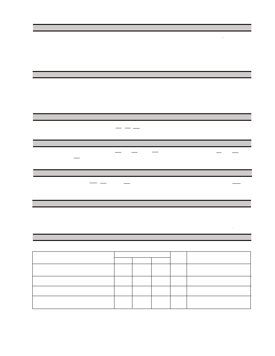
ERASE AND PROGRAMMING PERFORMANCE
Sector Erase Time
-
1
15
sec
Excludes 00H programming
(Note 1)
prior to erasure.
Byte Programming Time
-
7
1000
us
Excludes System-level overhead.
Chip Programming Time
-
7.2
50
sec
Excludes system-level overhead.
(Note 1)
Chip Erase Time
-
16
240
sec
Exclude 00H programming
(Note 1)
prior to erase
Limits
Parameter
Min
Typ
Max
Unit
Comments
Notes: (1) 25OC, 5V V
CC, 100,000 cycles.
(Note 1)
相关PDF资料 |
PDF描述 |
|---|---|
| PUMA68F4001MB-15 | 128K X 32 FLASH 5V PROM MODULE, 150 ns, PQMA68 |
| PUMA68S16000XBL-012 | 512K X 32 MULTI DEVICE SRAM MODULE, 12 ns, PQCC68 |
| PUMA68SV16000B-020 | 512K X 32 MULTI DEVICE SRAM MODULE, 20 ns, PQMA68 |
| PUMA68SV16000B-35 | 512K X 32 MULTI DEVICE SRAM MODULE, 35 ns, PQMA68 |
| PUMA77FV16006AM-90E | 256 CABGA, IND TEMP(FPGA) |
相关代理商/技术参数 |
参数描述 |
|---|---|
| PUMA68F32006X-12 | 制造商:未知厂家 制造商全称:未知厂家 功能描述:EEPROM |
| PUMA68F32006X-15 | 制造商:未知厂家 制造商全称:未知厂家 功能描述:EEPROM |
| PUMA68F32006X-90 | 制造商:未知厂家 制造商全称:未知厂家 功能描述:EEPROM |
| PUMA68F32006XI-12 | 制造商:未知厂家 制造商全称:未知厂家 功能描述:EEPROM |
| PUMA68F32006XI-15 | 制造商:未知厂家 制造商全称:未知厂家 功能描述:EEPROM |
发布紧急采购,3分钟左右您将得到回复。