- 您现在的位置:买卖IC网 > PDF目录299793 > PUMA68F32006M-90E 1M X 32 FLASH 5V PROM MODULE, 90 ns, PQMA68 PDF资料下载
参数资料
| 型号: | PUMA68F32006M-90E |
| 元件分类: | PROM |
| 英文描述: | 1M X 32 FLASH 5V PROM MODULE, 90 ns, PQMA68 |
| 封装: | PLASTIC, LCC-68 |
| 文件页数: | 5/23页 |
| 文件大小: | 181K |
| 代理商: | PUMA68F32006M-90E |
13
PUMA 68F32006/A-90/12/15
Issue 4.2 : December 1999
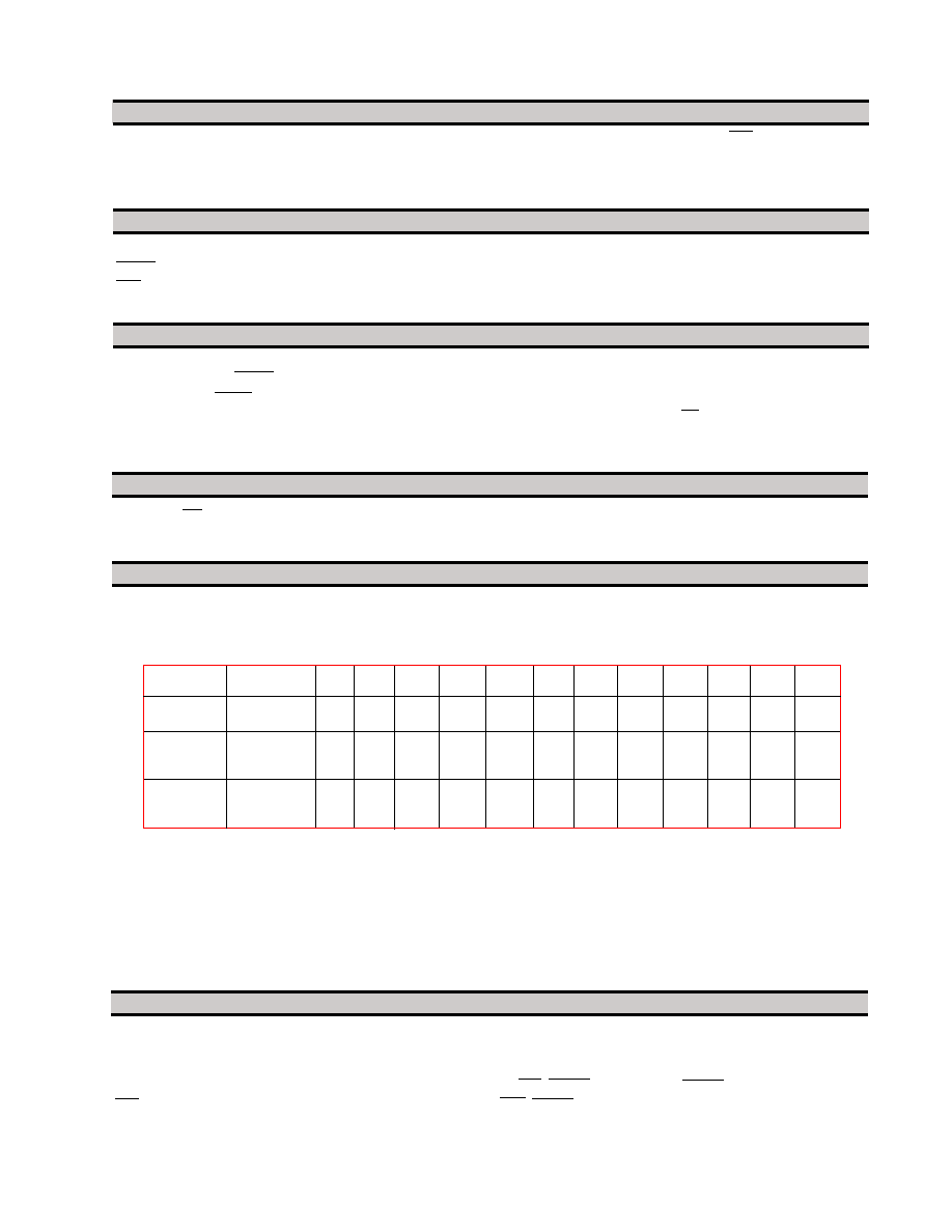
Type
A17-A19
A6
A1
A0
Code
DQ7
DQ6
DQ5
DQ4
DQ3
DQ2
DQ1
DQ0
Manufacture
X
V
IL
V
IL
V
IL
01H
0
0000
001
Code
X
V
IL
V
IL
V
IH
A4H
1
1010
101
Device Code
Sector Group Sector Group
V
IL
V
IH
V
IL
01H*
0
0000
001
Protection
Address
DEVICE OPERATION
The autoselect mode allows the reading out of a binary code from the device and will identify the die manu-
facturer and type. This mode is intended for use by programming equipment. This mode is functional over the
full military temperature range. The autoselect codes for the first device are as follows :
Autoselect
To activate this mode the programming equipment must force V
ID on address A9 . Two identifier bytes may
then be sequenced from each die device outputs by toggling A0 from V
IL to VIH. All addresses are dont care
apart from A0, A1, A6. All identifiers for manufacturer and device will exhibit odd parity with D7 defined as the
parity bit. In order to read the proper device codes when executing the autoselect A1 must be V
IL.
The device has two control functions which must be satisfied in order to obtain data at the outputs
CE1-4 is the power control and should be used for device selection
OE is the output control and should be used to gate data to the output pins if the device is selected.
Read Mode
Two standby modes are available :
CMOS standby : CE1-4 held at Vcc +/- 0.3V
TTL standby : CE1-4 held at V
IH
In the standby mode the outputs are in a high impedance state independent of the OE input. If the device is
deselected during erasure or programming the device will draw active current until the operation is completed.
Standby Mode
With the OE input at a logic high level (V
IH), output from the device is disabled. This will cause the output pins
to be in a high impedance state.
Output Disable
Device erasure and programming are accomplished via the command register. The contents of the register
serve as inputs to the internal state machine. The state machine outputs dictate the function of the device. The
register is a latch used to store the commands along with the address and data information required to execute
the command. The command register is written by bringing WE/WE1-4 to V
IL while CE1-4 is at VIL and
OE is at V
IH.Addresses are latched on the falling edge of WE/WE1-4 while data is latched on the rising edge.
Write
The following description deals with the device operating in 8 bit mode accessed through CE1,
however status flag definitions shown apply equally to the corresponding flag for each device in the module.
(HEX)
* Outputs 01H at protected sector address
相关PDF资料 |
PDF描述 |
|---|---|
| PUMA68F4001MB-15 | 128K X 32 FLASH 5V PROM MODULE, 150 ns, PQMA68 |
| PUMA68S16000XBL-012 | 512K X 32 MULTI DEVICE SRAM MODULE, 12 ns, PQCC68 |
| PUMA68SV16000B-020 | 512K X 32 MULTI DEVICE SRAM MODULE, 20 ns, PQMA68 |
| PUMA68SV16000B-35 | 512K X 32 MULTI DEVICE SRAM MODULE, 35 ns, PQMA68 |
| PUMA77FV16006AM-90E | 256 CABGA, IND TEMP(FPGA) |
相关代理商/技术参数 |
参数描述 |
|---|---|
| PUMA68F32006X-12 | 制造商:未知厂家 制造商全称:未知厂家 功能描述:EEPROM |
| PUMA68F32006X-15 | 制造商:未知厂家 制造商全称:未知厂家 功能描述:EEPROM |
| PUMA68F32006X-90 | 制造商:未知厂家 制造商全称:未知厂家 功能描述:EEPROM |
| PUMA68F32006XI-12 | 制造商:未知厂家 制造商全称:未知厂家 功能描述:EEPROM |
| PUMA68F32006XI-15 | 制造商:未知厂家 制造商全称:未知厂家 功能描述:EEPROM |
发布紧急采购,3分钟左右您将得到回复。