参数资料
| 型号: | QLX4300SIQSR |
| 厂商: | Intersil |
| 文件页数: | 3/21页 |
| 文件大小: | 0K |
| 描述: | IC EQUALIZER REC 3.125GBPS 46QFN |
| 标准包装: | 100 |
| 系列: | QLx™ |
| 应用: | 数据传输 |
| 接口: | SMBus(2 线/I²C) |
| 电源电压: | 1.1 V ~ 1.3 V |
| 封装/外壳: | 46-WFQFN 裸露焊盘 |
| 供应商设备封装: | 46-TQFN |
| 包装: | 带卷 (TR) |
| 安装类型: | 表面贴装 |
11
FN6982.1
November 19, 2009
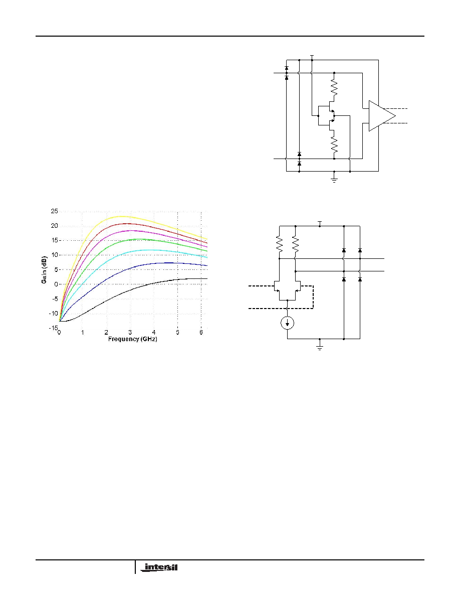
the boost level and one of 18 compensation levels when
the CP[k] pins are used to set the level. The equalizer
transfer functions for a subset of these compensation
levels are plotted in Figure 18. The flexibility of this
adjustable compensation architecture enables signal
fidelity to be optimized on a channel-by-channel basis,
providing support for a wide variety of channel
characteristics and data rates ranging from 2.5Gb/s to
3.125Gb/s. Because the boost level is externally set
rather than internally adapted, the QLx4300-S45
provides reliable communication from the very first bit
transmitted. There is no time needed for adaptation and
control loop convergence. Furthermore, there are no
pathological data patterns that will cause the
QLx4300-S45 to move to an incorrect boost level.
The “Applications Information” section beginning on
page 12 details how to set the boost level by both the
CP-pin voltage approach and the serial programming
approach.
CML Input and Output Buffers
The input and output buffers for the high-speed data
channels in the QLx4300-S45 are implemented using
CML. Equivalent input and output circuits are shown in
Line Silence/Electrical Idle/Quiescent Mode
Line silence is commonly broken by the limiting
amplification in other equalizers. This disruption can be
detrimental in many systems that rely on line silence as
part of the protocol. The QLx4300-S45 contains special
lane management capabilities to detect and preserve
periods of line silence while still providing the
fidelity-enhancing benefits of limiting amplification during
active data transmission. Line silence is detected by
measuring the amplitude of the equalized signal and
comparing that to a threshold set by the current at the
DT pin. When the amplitude falls below the threshold,
the output driver stages are muted and held at their
nominal common mode voltage1.
FIGURE 18. EQUALIZER TRANSFER FUNCTIONS FOR
SETTINGS 0, 5, 10, 15, 20, 25, AND 31 IN
THE QLx4300-S45
FIGURE 19. CML INPUT EQUIVALENT CIRCUIT FOR THE
QLx4300-S45
FIGURE 20. CML OUTPUT EQUIVALENT CIRCUIT FOR
THE QLx4300-S45
NOTE: The load value of 52Ω is used to internally match
SDD22 for a characteristic impedance of 50Ω.
1. The output common mode voltage remains constant during both active data transmission and output muting modes.
IN[k] P
IN[k] N
Buffer
VDD
50
VDD
52
OUT[k] P
OUT[k] N
QLx4300-S45
相关PDF资料 |
PDF描述 |
|---|---|
| QLX4600LIQSR | IC EQUALIZER REC 6.25GBPS 46QFN |
| QLX4600SIQSR | IC EQUALIZER REC 6.25GBPS 46QFN |
| R5F100GEAFB#V0 | MCU 16BIT 64KB FLASH 48LQFP |
| R5F2135CMNFP#V0 | IC MICROCONTROLLER |
| R5F562N8ADBG#U0 | MCU 32BIT FLASH 512KROM 176LFBGA |
相关代理商/技术参数 |
参数描述 |
|---|---|
| QLX4300SIQT7 | 功能描述:接口 - 专用 4 GBS QD CH LANE EXTENDER RoHS:否 制造商:Texas Instruments 产品类型:1080p60 Image Sensor Receiver 工作电源电压:1.8 V 电源电流:89 mA 最大功率耗散: 最大工作温度:+ 85 C 安装风格:SMD/SMT 封装 / 箱体:BGA-59 |
| QLX4600LIQSR | 功能描述:接口 - 专用 6 GBS QD CH LANE EXTENDER RoHS:否 制造商:Texas Instruments 产品类型:1080p60 Image Sensor Receiver 工作电源电压:1.8 V 电源电流:89 mA 最大功率耗散: 最大工作温度:+ 85 C 安装风格:SMD/SMT 封装 / 箱体:BGA-59 |
| QLX4600LIQT7 | 功能描述:接口 - 专用 6 GBS QD CH LANE EXTENDER RoHS:否 制造商:Texas Instruments 产品类型:1080p60 Image Sensor Receiver 工作电源电压:1.8 V 电源电流:89 mA 最大功率耗散: 最大工作温度:+ 85 C 安装风格:SMD/SMT 封装 / 箱体:BGA-59 |
| QLX4600MIBQ15 | 制造商:Intersil Corporation 功能描述:IC LINEAR |
| QLX4600-S30 | 制造商:INTERSIL 制造商全称:Intersil Corporation 功能描述:Quad Lane Extender |
发布紧急采购,3分钟左右您将得到回复。