- 您现在的位置:买卖IC网 > PDF目录11793 > QLX4600LIQT7 (Intersil)IC EQUALIZER REC 6.25GBPS 46QFN PDF资料下载
参数资料
| 型号: | QLX4600LIQT7 |
| 厂商: | Intersil |
| 文件页数: | 21/23页 |
| 文件大小: | 0K |
| 描述: | IC EQUALIZER REC 6.25GBPS 46QFN |
| 标准包装: | 1 |
| 系列: | QLx™ |
| 应用: | 铜电缆模块 |
| 电源电压: | 1.1 V ~ 1.3 V |
| 封装/外壳: | 46-WFQFN 裸露焊盘 |
| 供应商设备封装: | 46-TQFN |
| 包装: | 标准包装 |
| 安装类型: | 表面贴装 |
| 其它名称: | QLX4600LIQT7-DKR QLX4600LIQT7-DKR-ND QLX4600LIQT7DKR |
7
FN6981.1
November 19, 2009
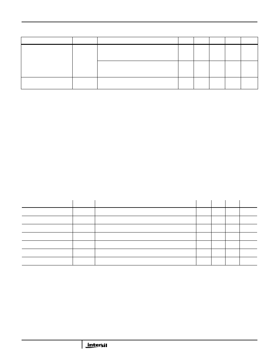
Line Silence-to-Data
Response Time
tSD
Time to transition from line silence mode
(muted output) to active data on 20m
24AWG standard twin-axial cable at 5Gb/s
20
ns
Time from first bit of ALIGN(0) for SAS
OOB signaling to 450mVP-P output;
Meritec 24AWG 20m; 3Gb/s
19
ns
Timing Difference (SAS)
|t DS - t SD| For SAS OOB signaling support; Meritec
24AWG 20m
5ns
NOTES:
3. After channel loss, differential amplitudes at QLx4600-SL30 inputs must meet the input voltage range specified in “Absolute
4. Temperature = +25°C, VDD = 1.2V.
5. Output residual jitter is the difference between the total jitter at the lane extender output and the total jitter of the transmitted
signal (as measured at the input to the channel). Total jitter (TJ) is DJPP + 14.1 x RJRMS.
6. Measured using a PRBS 27-1 pattern. Deterministic jitter at the input to the lane extender is due to frequency-dependent,
media-induced loss only.
7. Rise and fall times measured using a 1GHz clock with a 20ps edge rate.
8. For active data mode, cable input amplitude is 400mVP-P (differential) or greater. For line silence mode, cable input amplitude
is 20mVP-P (differential) or less.
9. Measured differentially across the data source.
10. During line silence, transmitter noise in excess of this voltage range may result in differential output amplitudes from the
QLx4600 that are greater than 20mVP-P.
11. The data pattern preceding line silence mode is comprised of the PCIe electrical idle ordered set (EIOS). The data pattern
following line silence mode is comprised of the PCIe electrical idle exit sequence (EIES).
12. The data pattern preceding or following line silence mode is comprised of the SAS-2 ALIGN (0) sequence for OOB signaling at
3Gb/s, and amplitude of 800mVP-P.
Electrical Specifications Typical values are at VDD = 1.2V, TA = +25°C, and VIN = 800mVP-P, unless otherwise noted.
VDD = 1.1V to 1.3V, TA = 0°C to +70°C. (Continued)
PARAMETERS
SYMBOL
CONDITION
MIN
TYP
MAX
UNITS NOTES
Serial Bus Timing Characteristics
PARAMETER
SYMBOL
CONDITION
MIN
TYP
MAX
UNITS
CLK Setup Time
tSCK
From the falling edge of ENB
10
ns
DI Setup Time
tSDI
Prior to the rising edge of CLK
10
ns
DI Hold Time
tHDI
From the rising edge of CLK
6
ns
ENB ‘HIGH’
tHEN
From the falling edge of the last data bit’s CLK
10
ns
Boost Setting Operational
tD
From ENB ‘HIGH’
10
ns
DO Hold Time
tCQ
From the rising edge of CLK to DO transition
12
ns
Clock Rate
fCLK
Reference clock for serial bus EQ programming
20
MHz
QLx4600-SL30
相关PDF资料 |
PDF描述 |
|---|---|
| QLX4600SIQT7 | IC EQUALIZER REC 6.25GBPS 46QFN |
| DS80C310-QCG+ | IC MCU HI SPEED 25MHZ 44-PLCC |
| QLX4300SIQT7 | IC EQUALIZER REC 3.125GBPS 46QFN |
| AT32UC3A3128-ALUR | IC MCU 128KB FLASH 144LQFP |
| AT32UC3C2256C-A2UR | IC MCU AVR32 256K FLASH 64TQFP |
相关代理商/技术参数 |
参数描述 |
|---|---|
| QLX4600MIBQ15 | 制造商:Intersil Corporation 功能描述:IC LINEAR |
| QLX4600-S30 | 制造商:INTERSIL 制造商全称:Intersil Corporation 功能描述:Quad Lane Extender |
| QLX4600SIQSR | 功能描述:接口 - 专用 6 GBS QD CH LANE EXTENDER RoHS:否 制造商:Texas Instruments 产品类型:1080p60 Image Sensor Receiver 工作电源电压:1.8 V 电源电流:89 mA 最大功率耗散: 最大工作温度:+ 85 C 安装风格:SMD/SMT 封装 / 箱体:BGA-59 |
| QLX4600SIQT7 | 功能描述:接口 - 专用 6 GBS QD CH LANE EXTENDER RoHS:否 制造商:Texas Instruments 产品类型:1080p60 Image Sensor Receiver 工作电源电压:1.8 V 电源电流:89 mA 最大功率耗散: 最大工作温度:+ 85 C 安装风格:SMD/SMT 封装 / 箱体:BGA-59 |
| QLX4600-SL30 | 制造商:INTERSIL 制造商全称:Intersil Corporation 功能描述:Quad Lane Extender |
发布紧急采购,3分钟左右您将得到回复。