- 您现在的位置:买卖IC网 > PDF目录11793 > QLX4600LIQT7 (Intersil)IC EQUALIZER REC 6.25GBPS 46QFN PDF资料下载
参数资料
| 型号: | QLX4600LIQT7 |
| 厂商: | Intersil |
| 文件页数: | 6/23页 |
| 文件大小: | 0K |
| 描述: | IC EQUALIZER REC 6.25GBPS 46QFN |
| 标准包装: | 1 |
| 系列: | QLx™ |
| 应用: | 铜电缆模块 |
| 电源电压: | 1.1 V ~ 1.3 V |
| 封装/外壳: | 46-WFQFN 裸露焊盘 |
| 供应商设备封装: | 46-TQFN |
| 包装: | 标准包装 |
| 安装类型: | 表面贴装 |
| 其它名称: | QLX4600LIQT7-DKR QLX4600LIQT7-DKR-ND QLX4600LIQT7DKR |
14
FN6981.1
November 19, 2009
The boost setting for equalizer channel k can be read as
a three digit ternary number across CP[k][A,B,C]. The
ternary value is established by the value of the resistor
between VDD and the CP[k][A,B,C] pin.
As a second option, the equalizer boost setting can be
taken from a set of registers programmed through a
serial bus interface (pins 16, 17, 45, and 46). Using this
interface, a set of registers is programmed to store the
boost level. A total of 21 registers are used. Registers 2
through 21 are parsed into four 5-bit words. Each 5-bit
word determines which of 32 boost levels to use for the
corresponding equalizer. Register 1 instructs the
QLx4600-SL30 to use registers 2 through 21 to set the
boost level rather than the control pins CP[k][A,B,C].
Both options have their relative advantages. The control
pin option minimizes the need for external controllers as
the boost level can be set in the board design resulting in
a compact layout. The register option is more flexible for
cases in which the optimum boost level will not be known
and can be changed by a host bus adapter with a small
number of pins. It is noted that the serial bus interface
can also be daisy-chained among multiple QLx4600-SL30
devices to afford a compact programmable solution even
when a large number of data lines need to be equalized.
Upon power-up, the default value of all the registers (and
register 1 in particular) is zero, and thus, the CP pins are
used to set the boost level. This permits an alternate
interpretation on setting the boost level. Specifically, the
CP pins define the default boost level until the registers
are (if ever) programmed via the serial bus.
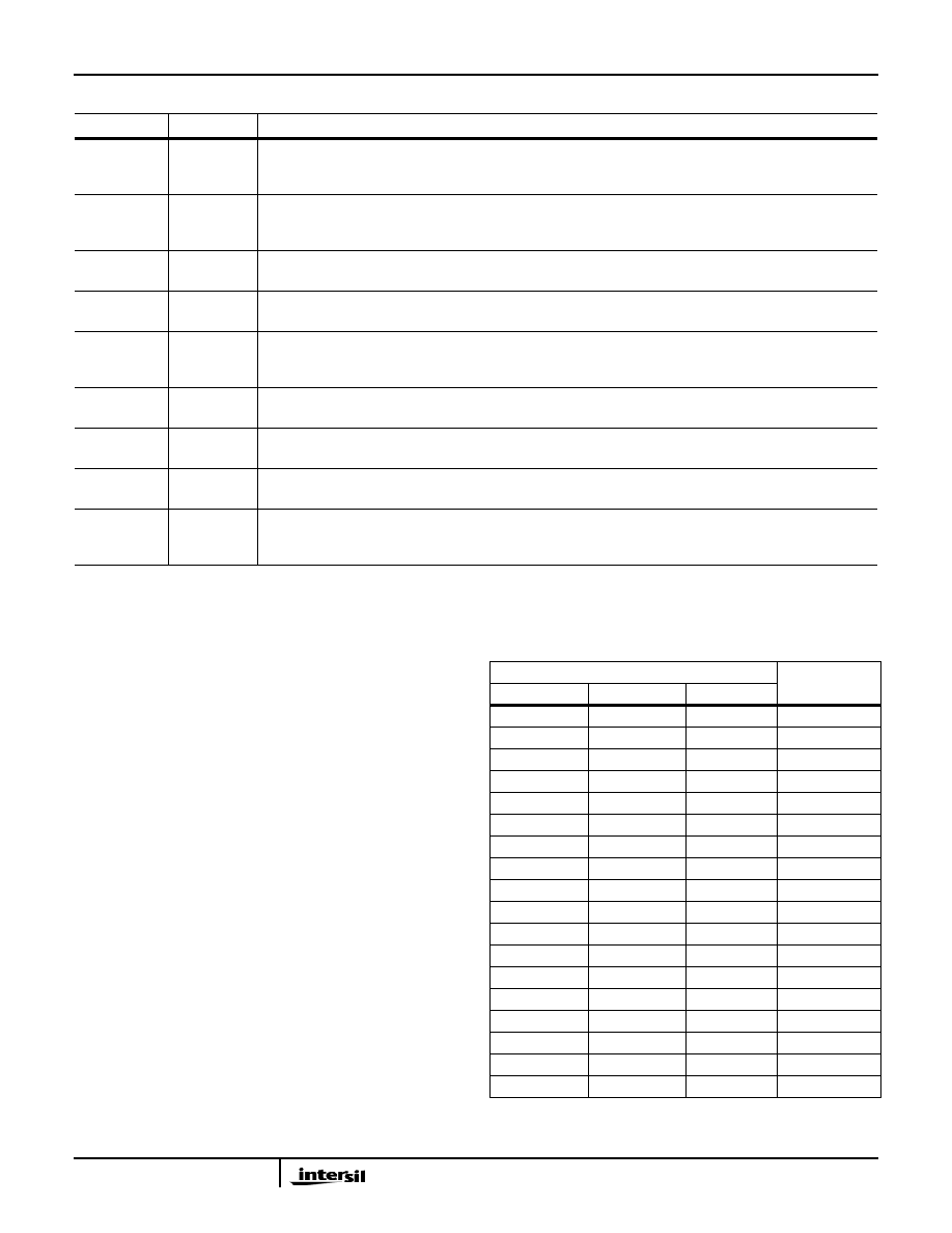
TABLE 1. DESCRIPTIONS OF PINS USED TO SET EQUALIZATION BOOST LEVEL
PIN NAME
PIN NUMBER DESCRIPTION
DI
16
Serial data input, CMOS logic. Input for serial data stream to program internal registers controlling
the boost for all four equalizers. Synchronized with clock (CLK) on pin 46. Overrides the boost
setting established on CP control pins. Internally pulled down.
DO
17
Serial data output, CMOS logic. Output of the internal registers controlling the boost for all four
equalizers. Synchronized with clock on pin 46. Equivalent to serial data input on DI but delayed by
21 clock cycles.
CP3[A,B,C]
18, 19, 20
Control pins for setting equalizer 3. CMOS logic inputs. Pins are read as a 3-digit number to set the
boost level. A is the MSB, and C is the LSB. Pins are internally pulled down through a 25kΩ resistor.
CP4[A,B,C]
21, 22, 23
Control pins for setting equalizer 4. CMOS logic inputs. Pins are read as a 3-digit number to set the
boost level. A is the MSB, and C is the LSB. Pins are internally pulled down through a 25kΩ resistor.
MODE
24
Boost-level control mode input, CMOS logic. Allows serial programming of internal registers
through pins DI, ENB, and Clk when set HIGH. Resets all internal registers to zero and uses boost
levels set by CP pins when set LOW. If serial programming is not used, this pin should be grounded.
CP2[C,B,A]
39, 40, 41
Control pins for setting equalizer 2. CMOS logic inputs. Pins are read as a 3-digit number to set the
boost level. A is the MSB, and C is the LSB. Pins are internally pulled down through a 25kΩ resistor.
CP1[C,B,A]
42, 43, 44
Control pins for setting equalizer 1. CMOS logic inputs. Pins are read as a 3-digit number to set the
boost level. A is the MSB, and C is the LSB. Pins are internally pulled down through a 25kΩ resistor.
ENB
45
Serial data enable (active low), CMOS logic. Internal registers can be programmed with DI and CLK
pins only when the ENB pin is ‘LOW’. Internally pulled down.
CLK
46
Serial data clock, CMOS logic. Synchronous clock for serial data on DI and DO pins. Data on DI is
latched on the rising clock edge. Clock speed is recommended to be between 10MHz and 20MHz.
Internally pulled down.
TABLE 2. MAPPING BETWEEN CP-SETTING RESISTOR
AND PROGAMMED BOOST LEVELS
RESISTANCE BETWEEN CP PIN AND VDD
SERIAL
BOOST LEVEL
CP[A]
CP[B]
CP[C]
Open
0
Open
25kΩ
2
Open
0Ω
4
Open
25kΩ
Open
6
Open
25kΩ
8
Open
25kΩ
0Ω
10
Open
0Ω
Open
12
Open
0Ω
25kΩ
14
Open
0Ω
15
0Ω
Open
16
0Ω
Open
25kΩ
17
0Ω
Open
0Ω
19
0Ω
25kΩ
Open
21
0Ω
25kΩ
23
0Ω
25kΩ
0Ω
24
0Ω
Open
26
0Ω
25kΩ
28
0Ω
31
QLx4600-SL30
相关PDF资料 |
PDF描述 |
|---|---|
| QLX4600SIQT7 | IC EQUALIZER REC 6.25GBPS 46QFN |
| DS80C310-QCG+ | IC MCU HI SPEED 25MHZ 44-PLCC |
| QLX4300SIQT7 | IC EQUALIZER REC 3.125GBPS 46QFN |
| AT32UC3A3128-ALUR | IC MCU 128KB FLASH 144LQFP |
| AT32UC3C2256C-A2UR | IC MCU AVR32 256K FLASH 64TQFP |
相关代理商/技术参数 |
参数描述 |
|---|---|
| QLX4600MIBQ15 | 制造商:Intersil Corporation 功能描述:IC LINEAR |
| QLX4600-S30 | 制造商:INTERSIL 制造商全称:Intersil Corporation 功能描述:Quad Lane Extender |
| QLX4600SIQSR | 功能描述:接口 - 专用 6 GBS QD CH LANE EXTENDER RoHS:否 制造商:Texas Instruments 产品类型:1080p60 Image Sensor Receiver 工作电源电压:1.8 V 电源电流:89 mA 最大功率耗散: 最大工作温度:+ 85 C 安装风格:SMD/SMT 封装 / 箱体:BGA-59 |
| QLX4600SIQT7 | 功能描述:接口 - 专用 6 GBS QD CH LANE EXTENDER RoHS:否 制造商:Texas Instruments 产品类型:1080p60 Image Sensor Receiver 工作电源电压:1.8 V 电源电流:89 mA 最大功率耗散: 最大工作温度:+ 85 C 安装风格:SMD/SMT 封装 / 箱体:BGA-59 |
| QLX4600-SL30 | 制造商:INTERSIL 制造商全称:Intersil Corporation 功能描述:Quad Lane Extender |
发布紧急采购,3分钟左右您将得到回复。