- 您现在的位置:买卖IC网 > PDF目录191949 > QS5930-50TQ (INTEGRATED DEVICE TECHNOLOGY INC) 5930 SERIES, PLL BASED CLOCK DRIVER, 6 TRUE OUTPUT(S), 0 INVERTED OUTPUT(S), PDSO20 PDF资料下载
参数资料
| 型号: | QS5930-50TQ |
| 厂商: | INTEGRATED DEVICE TECHNOLOGY INC |
| 元件分类: | Clock Driver |
| 英文描述: | 5930 SERIES, PLL BASED CLOCK DRIVER, 6 TRUE OUTPUT(S), 0 INVERTED OUTPUT(S), PDSO20 |
| 封装: | QSOP-20 |
| 文件页数: | 2/6页 |
| 文件大小: | 67K |
| 代理商: | QS5930-50TQ |
2
INDUSTRIALTEMPERATURERANGE
QS5930T
LOW SKEW CMOS PLL CLOCK DRIVER WITH INTEGRATED LOOP FILTER
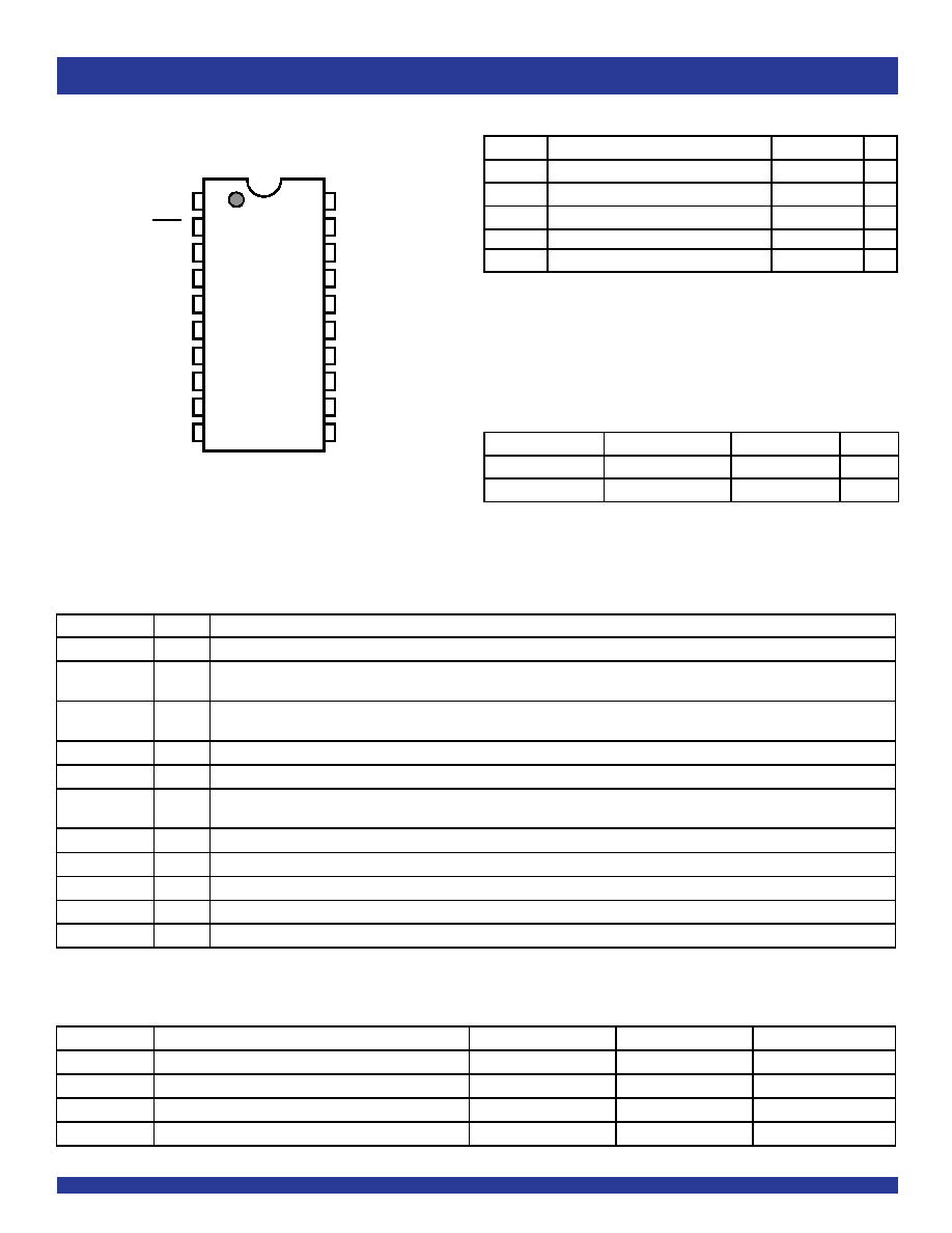
PIN CONFIGURATION
QSOP
TOP VIEW
1
2
3
4
5
6
7
8
9
10
20
19
18
17
16
15
14
13
12
11
GND
OE/RST
FEEDBACK
AVDD
AGND
SYNC
FREQ_SEL
GND
Q0
Q4
Q/2
GND
Q3
Q2
GND
PLL_EN
GND
Q1
VDD
ABSOLUTE MAXIMUM RATINGS (1)
Symbol
Rating
Max.
Unit
AVDD,VDD Supply Voltage to Ground
–0.5 to +7
V
DC Input Voltage VIN
–0.5 to +7
V
AC Input Voltage (for pulse width
≤ 20ns)
–3
V
Maximum Power Dissipation (TA = 85°C)
1
W
TSTG
Storage Temperature Range
–65 to +150
°C
NOTE:
1. Stresses greater than those listed under ABSOLUTE MAXIMUM
RATINGS may cause permanent damage to the device. This is a
stress rating only and functional operation of the device at these or
any other conditions above those indicated in the operational sections
of this specification is not implied. Exposure to absolute maximum
rating conditions for extended periods may affect reliability.
CAPACITANCE (T
A
= 25
° C, f = 1MHz, VIN = 0V)
Pins
Typ.
Max.
Unit
CIN
34
pF
COUT
79
pF
PIN DESCRIPTION
Pin Name
I/O
Description
SYNC
I
Reference clock input
FREQ_SEL
I
VCO frequency select. For choosing optimal VCO operating frequency depending on input frequency. HIGH is for higher
frequencies, LOW is for lower frequencies.
FEEDBACK
I
PLL feedback input which is connected to either a Q or a Q/2 output. External feedback provides flexibility for different output
frequency relationships. See the Frequency Selection Table for more information.
Q0 -Q4
O
Clock outputs
Q/2
O
Clock output. Matched in phase, but frequency is half the Q frequency.
OE/
RST
I
Output enable/asynchronous reset. Resets all output registers. When 0, all outputs are held in a tri-stated condition. When 1,
outputs are enabled.
PLL_EN
I
PLL enable. Enables and disables the PLL. Allows the SYNC input to be single-stepped for system debug.
VDD
—
Power supply for output buffers.
AVDD
—
Power supply for phase lock loop and other internal circuitries.
GND
—
Ground supply for output buffers.
AGND
—
Ground supply for phase lock loop and other internal circuitries.
OUTPUT FREQUENCY SPECIFICATIONS
Industrial: TA = –40°C to +85°C, AVDD/VDD = 5V ± 10%
Symbol
Description
– 50
– 66
Units
FMAX_Q
Max Frequency, Q0 - Q4,50
66
MHz
FMAX_Q/2
Max Frequency, Q/2
25
33
MHz
FMIN_Q
Min Frequency, Q0 - Q4
28
MHz
FMIN_Q/2
Min Frequency, Q/2
14
MHz
相关PDF资料 |
PDF描述 |
|---|---|
| QS5930-66TQ | 5930 SERIES, PLL BASED CLOCK DRIVER, 6 TRUE OUTPUT(S), 0 INVERTED OUTPUT(S), PDSO20 |
| QS762470-55J | 1 CHANNEL(S), LOCAL AREA NETWORK CONTROLLER, PQCC44 |
| QSC112.C4A0 | PHOTO TRANSISTOR DETECTOR |
| QSC114.C6A0 | PHOTO TRANSISTOR DETECTOR |
| QSD123.A4A0 | PHOTO TRANSISTOR DETECTOR |
相关代理商/技术参数 |
参数描述 |
|---|---|
| QS5930-66TQ | 制造商:Integrated Device Technology Inc 功能描述: |
| QS5930T | 制造商:IDT 制造商全称:Integrated Device Technology 功能描述:LOW SKEW CMOS PLL CLOCK DRIVER WITH INTEGRATED LOOP FILTER |
| QS5931-50Q | 制造商:未知厂家 制造商全称:未知厂家 功能描述:Six Distributed-Output Clock Driver |
| QS5931-66Q | 制造商:未知厂家 制造商全称:未知厂家 功能描述:Six Distributed-Output Clock Driver |
| QS5931-80Q | 制造商:未知厂家 制造商全称:未知厂家 功能描述:Six Distributed-Output Clock Driver |
发布紧急采购,3分钟左右您将得到回复。