- 您现在的位置:买卖IC网 > PDF目录230911 > R5F3650KNFA MICROCONTROLLER, PQFP100 PDF资料下载
参数资料
| 型号: | R5F3650KNFA |
| 元件分类: | 微控制器/微处理器 |
| 英文描述: | MICROCONTROLLER, PQFP100 |
| 封装: | 20 X 14 MM, 0.65 MM PITCH, QFP-100 |
| 文件页数: | 45/81页 |
| 文件大小: | 879K |
| 代理商: | R5F3650KNFA |
第1页第2页第3页第4页第5页第6页第7页第8页第9页第10页第11页第12页第13页第14页第15页第16页第17页第18页第19页第20页第21页第22页第23页第24页第25页第26页第27页第28页第29页第30页第31页第32页第33页第34页第35页第36页第37页第38页第39页第40页第41页第42页第43页第44页当前第45页第46页第47页第48页第49页第50页第51页第52页第53页第54页第55页第56页第57页第58页第59页第60页第61页第62页第63页第64页第65页第66页第67页第68页第69页第70页第71页第72页第73页第74页第75页第76页第77页第78页第79页第80页第81页
63
4317K–AVR–03/2013
AT90PWM2/3/2B/3B
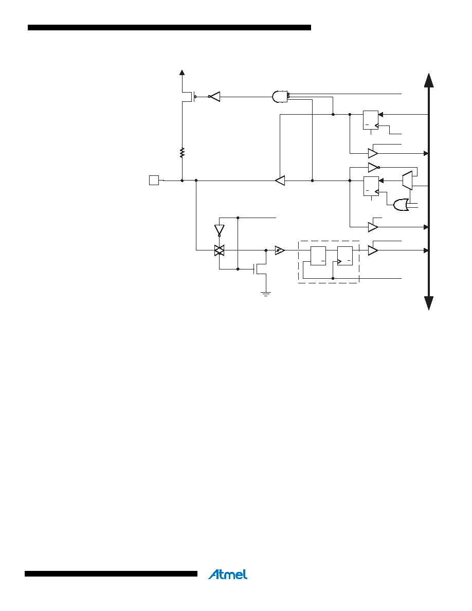
Figure 11-2. General Digital I/O
Note:
1. WRx, WPx, WDx, RRx, RPx, and RDx are common to all pins within the same port. clk
I/O,
SLEEP, and PUD are common to all ports.
11.2.1
Configuring the Pin
Each port pin consists of three register bits: DDxn, PORTxn, and PINxn. As shown in “Register
Description for I/O-Ports” on page 80, the DDxn bits are accessed at the DDRx I/O address, the
PORTxn bits at the PORTx I/O address, and the PINxn bits at the PINx I/O address.
The DDxn bit in the DDRx Register selects the direction of this pin. If DDxn is written logic one,
Pxn is configured as an output pin. If DDxn is written logic zero, Pxn is configured as an input
pin.
If PORTxn is written logic one when the pin is configured as an input pin, the pull-up resistor is
activated. To switch the pull-up resistor off, PORTxn has to be written logic zero or the pin has to
be configured as an output pin
The port pins are tri-stated when reset condition becomes active, even if no clocks are running.
If PORTxn is written logic one when the pin is configured as an output pin, the port pin is driven
high (one). If PORTxn is written logic zero when the pin is configured as an output pin, the port
pin is driven low (zero).
clk
RPx
RRx
RDx
WDx
PUD
SYNCHRONIZER
WDx: WRITE DDRx
WRx: WRITE PORTx
RRx:
READ PORTx REGISTER
RPx:
READ PORTx PIN
PUD: PULLUP DISABLE
clk
I/O : I/O CLOCK
RDx:
READ DDRx
D
L
Q
RESET
Q
D
Q
D
CLR
PORTxn
Q
D
CLR
DDxn
PINxn
D
ATA
B
U
S
SLEEP
SLEEP: SLEEP CONTROL
Pxn
I/O
WPx
0
1
WRx
WPx: WRITE PINx REGISTER
相关PDF资料 |
PDF描述 |
|---|---|
| R5F3650MDFB | MICROCONTROLLER, PQFP100 |
| R5F3650NDFB | MICROCONTROLLER, PQFP100 |
| R5F3650RNFB | MICROCONTROLLER, PQFP100 |
| R5F3651ENFC | MICROCONTROLLER, PQFP128 |
| R5F3651KDFC | MICROCONTROLLER, PQFP128 |
相关代理商/技术参数 |
参数描述 |
|---|---|
| R5F3650KNFA#U0 | 功能描述:MCU 4KB FLASH 384/16K 100-QFP RoHS:是 类别:集成电路 (IC) >> 嵌入式 - 微控制器, 系列:M16C™ M16C/60/65 产品培训模块:CAN Basics Part-1 CAN Basics Part-2 Electromagnetic Noise Reduction Techniques Part 1 M16C Product Overview Part 1 M16C Product Overview Part 2 标准包装:1 系列:M16C™ M32C/80/87 核心处理器:M32C/80 芯体尺寸:16/32-位 速度:32MHz 连通性:EBI/EMI,I²C,IEBus,IrDA,SIO,UART/USART 外围设备:DMA,POR,PWM,WDT 输入/输出数:121 程序存储器容量:384KB(384K x 8) 程序存储器类型:闪存 EEPROM 大小:- RAM 容量:24K x 8 电压 - 电源 (Vcc/Vdd):3 V ~ 5.5 V 数据转换器:A/D 34x10b,D/A 2x8b 振荡器型:内部 工作温度:-20°C ~ 85°C 封装/外壳:144-LQFP 包装:托盘 产品目录页面:749 (CN2011-ZH PDF) 配用:R0K330879S001BE-ND - KIT DEV RSK M32C/87 |
| R5F3650KNFB | 制造商:RENESAS 制造商全称:Renesas Technology Corp 功能描述:This MCU consumes low power, and supports operating modes |
| R5F3650KNFB#U0 | 功能描述:MCU 4KB FLASH 384/16K 100-LQFP RoHS:是 类别:集成电路 (IC) >> 嵌入式 - 微控制器, 系列:M16C™ M16C/60/65 标准包装:96 系列:PIC® 16F 核心处理器:PIC 芯体尺寸:8-位 速度:20MHz 连通性:I²C,SPI 外围设备:欠压检测/复位,POR,PWM,WDT 输入/输出数:11 程序存储器容量:3.5KB(2K x 14) 程序存储器类型:闪存 EEPROM 大小:- RAM 容量:128 x 8 电压 - 电源 (Vcc/Vdd):2.3 V ~ 5.5 V 数据转换器:A/D 8x10b 振荡器型:内部 工作温度:-40°C ~ 125°C 封装/外壳:14-TSSOP(0.173",4.40mm 宽) 包装:管件 |
| R5F3650MCDFA | 制造商:RENESAS 制造商全称:Renesas Technology Corp 功能描述:televisions, household appliances, office equipment, communication devices |
| R5F3650MCDFB | 制造商:RENESAS 制造商全称:Renesas Technology Corp 功能描述:televisions, household appliances, office equipment, communication devices |
发布紧急采购,3分钟左右您将得到回复。