- 您现在的位置:买卖IC网 > PDF目录230911 > R5F3650KNFA MICROCONTROLLER, PQFP100 PDF资料下载
参数资料
| 型号: | R5F3650KNFA |
| 元件分类: | 微控制器/微处理器 |
| 英文描述: | MICROCONTROLLER, PQFP100 |
| 封装: | 20 X 14 MM, 0.65 MM PITCH, QFP-100 |
| 文件页数: | 72/81页 |
| 文件大小: | 879K |
| 代理商: | R5F3650KNFA |
第1页第2页第3页第4页第5页第6页第7页第8页第9页第10页第11页第12页第13页第14页第15页第16页第17页第18页第19页第20页第21页第22页第23页第24页第25页第26页第27页第28页第29页第30页第31页第32页第33页第34页第35页第36页第37页第38页第39页第40页第41页第42页第43页第44页第45页第46页第47页第48页第49页第50页第51页第52页第53页第54页第55页第56页第57页第58页第59页第60页第61页第62页第63页第64页第65页第66页第67页第68页第69页第70页第71页当前第72页第73页第74页第75页第76页第77页第78页第79页第80页第81页
90
4317K–AVR–03/2013
AT90PWM2/3/2B/3B
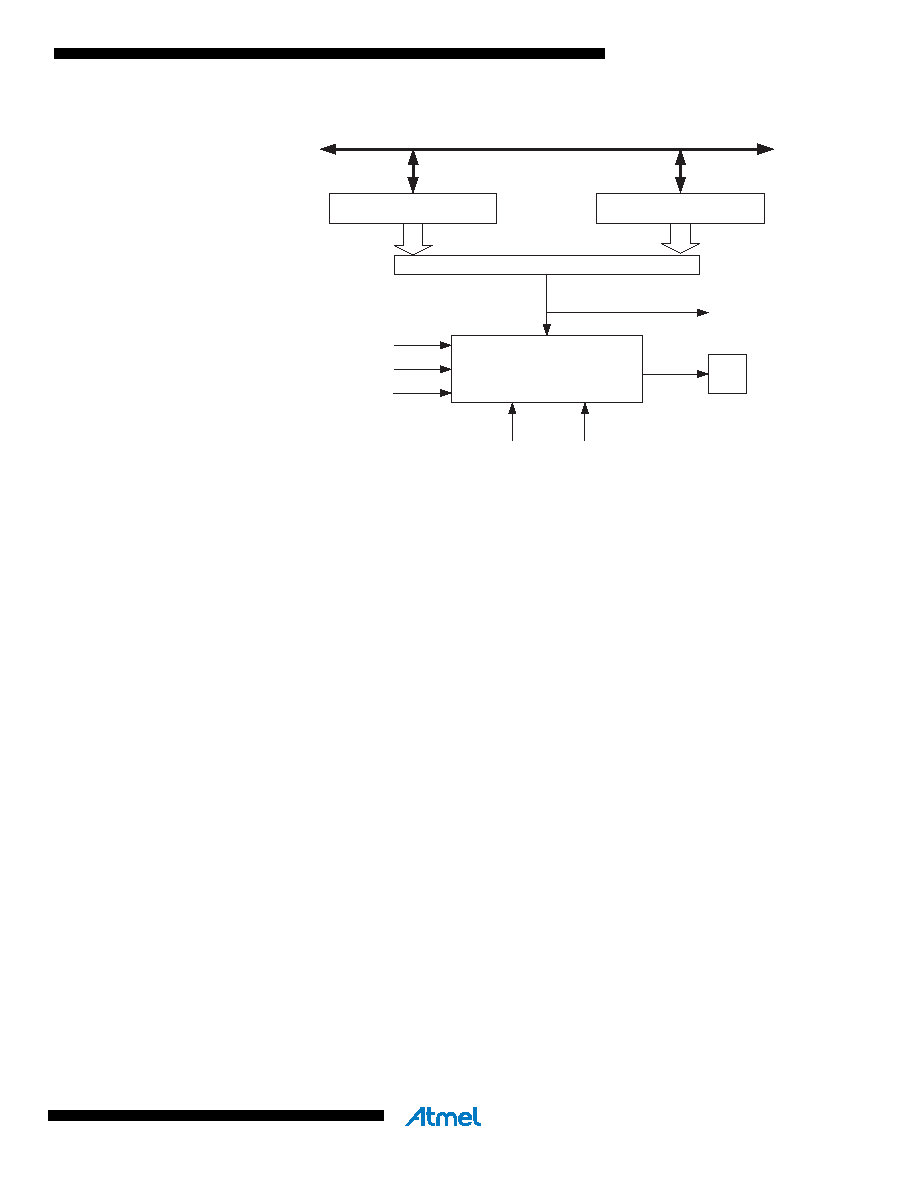
Figure 14-3. Output Compare Unit, Block Diagram
The OCR0x Registers are double buffered when using any of the Pulse Width Modulation
(PWM) modes. For the normal and Clear Timer on Compare (CTC) modes of operation, the dou-
ble buffering is disabled. The double buffering synchronizes the update of the OCR0x Compare
Registers to either top or bottom of the counting sequence. The synchronization prevents the
occurrence of odd-length, non-symmetrical PWM pulses, thereby making the output glitch-free.
The OCR0x Register access may seem complex, but this is not case. When the double buffering
is enabled, the CPU has access to the OCR0x Buffer Register, and if double buffering is dis-
abled the CPU will access the OCR0x directly.
14.4.1
Force Output Compare
In non-PWM waveform generation modes, the match output of the comparator can be forced by
writing a one to the Force Output Compare (FOC0x) bit. Forcing compare match will not set the
OCF0x Flag or reload/clear the timer, but the OC0x pin will be updated as if a real compare
match had occurred (the COM0x1:0 bits settings define whether the OC0x pin is set, cleared or
toggled).
14.4.2
Compare Match Blocking by TCNT0 Write
All CPU write operations to the TCNT0 Register will block any compare match that occur in the
next timer clock cycle, even when the timer is stopped. This feature allows OCR0x to be initial-
ized to the same value as TCNT0 without triggering an interrupt when the Timer/Counter clock is
enabled.
14.4.3
Using the Output Compare Unit
Since writing TCNT0 in any mode of operation will block all compare matches for one timer clock
cycle, there are risks involved when changing TCNT0 when using the Output Compare Unit,
independently of whether the Timer/Counter is running or not. If the value written to TCNT0
equals the OCR0x value, the compare match will be missed, resulting in incorrect waveform
generation. Similarly, do not write the TCNT0 value equal to BOTTOM when the counter is
downcounting.
OCFnx (Int.Req.)
= (8-bit Comparator )
OCRnx
OCnx
DATA BUS
TCNTn
WGMn1:0
Waveform Generator
top
FOCn
COMnx1:0
bottom
相关PDF资料 |
PDF描述 |
|---|---|
| R5F3650MDFB | MICROCONTROLLER, PQFP100 |
| R5F3650NDFB | MICROCONTROLLER, PQFP100 |
| R5F3650RNFB | MICROCONTROLLER, PQFP100 |
| R5F3651ENFC | MICROCONTROLLER, PQFP128 |
| R5F3651KDFC | MICROCONTROLLER, PQFP128 |
相关代理商/技术参数 |
参数描述 |
|---|---|
| R5F3650KNFA#U0 | 功能描述:MCU 4KB FLASH 384/16K 100-QFP RoHS:是 类别:集成电路 (IC) >> 嵌入式 - 微控制器, 系列:M16C™ M16C/60/65 产品培训模块:CAN Basics Part-1 CAN Basics Part-2 Electromagnetic Noise Reduction Techniques Part 1 M16C Product Overview Part 1 M16C Product Overview Part 2 标准包装:1 系列:M16C™ M32C/80/87 核心处理器:M32C/80 芯体尺寸:16/32-位 速度:32MHz 连通性:EBI/EMI,I²C,IEBus,IrDA,SIO,UART/USART 外围设备:DMA,POR,PWM,WDT 输入/输出数:121 程序存储器容量:384KB(384K x 8) 程序存储器类型:闪存 EEPROM 大小:- RAM 容量:24K x 8 电压 - 电源 (Vcc/Vdd):3 V ~ 5.5 V 数据转换器:A/D 34x10b,D/A 2x8b 振荡器型:内部 工作温度:-20°C ~ 85°C 封装/外壳:144-LQFP 包装:托盘 产品目录页面:749 (CN2011-ZH PDF) 配用:R0K330879S001BE-ND - KIT DEV RSK M32C/87 |
| R5F3650KNFB | 制造商:RENESAS 制造商全称:Renesas Technology Corp 功能描述:This MCU consumes low power, and supports operating modes |
| R5F3650KNFB#U0 | 功能描述:MCU 4KB FLASH 384/16K 100-LQFP RoHS:是 类别:集成电路 (IC) >> 嵌入式 - 微控制器, 系列:M16C™ M16C/60/65 标准包装:96 系列:PIC® 16F 核心处理器:PIC 芯体尺寸:8-位 速度:20MHz 连通性:I²C,SPI 外围设备:欠压检测/复位,POR,PWM,WDT 输入/输出数:11 程序存储器容量:3.5KB(2K x 14) 程序存储器类型:闪存 EEPROM 大小:- RAM 容量:128 x 8 电压 - 电源 (Vcc/Vdd):2.3 V ~ 5.5 V 数据转换器:A/D 8x10b 振荡器型:内部 工作温度:-40°C ~ 125°C 封装/外壳:14-TSSOP(0.173",4.40mm 宽) 包装:管件 |
| R5F3650MCDFA | 制造商:RENESAS 制造商全称:Renesas Technology Corp 功能描述:televisions, household appliances, office equipment, communication devices |
| R5F3650MCDFB | 制造商:RENESAS 制造商全称:Renesas Technology Corp 功能描述:televisions, household appliances, office equipment, communication devices |
发布紧急采购,3分钟左右您将得到回复。