- 您现在的位置:买卖IC网 > PDF目录230912 > R5F6411FDFN 32-BIT, FLASH, 50 MHz, MICROCONTROLLER, PQFP64 PDF资料下载
参数资料
| 型号: | R5F6411FDFN |
| 元件分类: | 微控制器/微处理器 |
| 英文描述: | 32-BIT, FLASH, 50 MHz, MICROCONTROLLER, PQFP64 |
| 封装: | 10 X 10 MM, 0.50 MM PITCH, PLASTIC, LQFP-64 |
| 文件页数: | 69/84页 |
| 文件大小: | 1206K |
| 代理商: | R5F6411FDFN |
第1页第2页第3页第4页第5页第6页第7页第8页第9页第10页第11页第12页第13页第14页第15页第16页第17页第18页第19页第20页第21页第22页第23页第24页第25页第26页第27页第28页第29页第30页第31页第32页第33页第34页第35页第36页第37页第38页第39页第40页第41页第42页第43页第44页第45页第46页第47页第48页第49页第50页第51页第52页第53页第54页第55页第56页第57页第58页第59页第60页第61页第62页第63页第64页第65页第66页第67页第68页当前第69页第70页第71页第72页第73页第74页第75页第76页第77页第78页第79页第80页第81页第82页第83页第84页
85
ATmega48PA/88PA/168PA [DATASHEET]
9223F–AVR–04/14
15.5.3 Using the Output Compare Unit
Since writing TCNT0 in any mode of operation will block all compare matches for one timer clock cycle, there are risks
involved when changing TCNT0 when using the output compare Unit, independently of whether the Timer/Counter is
running or not. If the value written to TCNT0 equals the OCR0x value, the compare match will be missed, resulting in
incorrect waveform generation. Similarly, do not write the TCNT0 value equal to BOTTOM when the counter is
downcounting.
The setup of the OC0x should be performed before setting the data Direction register for the port pin to output. The easiest
way of setting the OC0x value is to use the force output compare (FOC0x) strobe bits in normal mode. The OC0x registers
keep their values even when changing between waveform generation modes.
Be aware that the COM0x1:0 bits are not double buffered together with the compare value. Changing the COM0x1:0 bits will
take effect immediately.
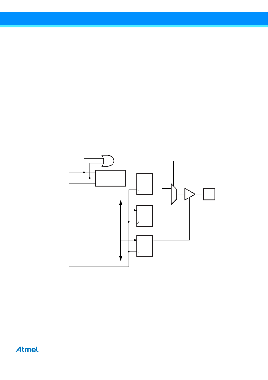
15.6
Compare Match Output Unit
The compare output mode (COM0x1:0) bits have two functions. The waveform generator uses the COM0x1:0 bits for
defining the output compare (OC0x) state at the next compare match. Also, the COM0x1:0 bits control the OC0x pin output
source. Figure 15-4 shows a simplified schematic of the logic affected by the COM0x1:0 bit setting. The I/O registers,
I/O bits, and I/O pins in the figure are shown in bold. Only the parts of the general I/O port control registers (DDR and PORT)
that are affected by the COM0x1:0 bits are shown. When referring to the OC0x state, the reference is for the internal OC0x
register, not the OC0x pin. If a system reset occur, the OC0x register is reset to “0”.
Figure 15-4. Compare Match Output Unit, Schematic
The general I/O port function is overridden by the output compare (OC0x) from the waveform generator if either of the
COM0x1:0 bits are set. However, the OC0x pin direction (input or output) is still controlled by the data direction register
(DDR) for the port pin. The data direction register bit for the OC0x pin (DDR_OC0x) must be set as output before the OC0x
value is visible on the pin. The port override function is independent of the waveform generation mode.
The design of the output compare pin logic allows initialization of the OC0x state before the output is enabled. Note that
some COM0x1:0 bit settings are reserved for certain modes of operation (see Section 15.9 “Register Description” on page
DA
T
A
BUS
0
1
Q
D
COMnx1
COMnx0
FOCn
OCnx
Waveform
Generator
Q
D
PORT
Q
D
DDR
OCnx
Pin
clkI/O
相关PDF资料 |
PDF描述 |
|---|---|
| R5F6411FDFP | 32-BIT, FLASH, 50 MHz, MICROCONTROLLER, PQFP80 |
| R5F6411FDLG | 32-BIT, FLASH, 50 MHz, MICROCONTROLLER, PBGA100 |
| R5F6411FNFN | 32-BIT, FLASH, 50 MHz, MICROCONTROLLER, PQFP64 |
| R5F21366CDFA | 8-BIT, FLASH, 20 MHz, MICROCONTROLLER, PQFP64 |
| R5F21368FKFP | 32-BIT, FLASH, 20 MHz, MICROCONTROLLER, PQFP64 |
相关代理商/技术参数 |
参数描述 |
|---|---|
| R5F6411FDFN#UA | 功能描述:MCU 256+8KB FLASH 32K 64-LQFP RoHS:是 类别:集成电路 (IC) >> 嵌入式 - 微控制器, 系列:M16C/R32C/100/111 标准包装:96 系列:PIC® 16F 核心处理器:PIC 芯体尺寸:8-位 速度:20MHz 连通性:I²C,SPI 外围设备:欠压检测/复位,POR,PWM,WDT 输入/输出数:11 程序存储器容量:3.5KB(2K x 14) 程序存储器类型:闪存 EEPROM 大小:- RAM 容量:128 x 8 电压 - 电源 (Vcc/Vdd):2.3 V ~ 5.5 V 数据转换器:A/D 8x10b 振荡器型:内部 工作温度:-40°C ~ 125°C 封装/外壳:14-TSSOP(0.173",4.40mm 宽) 包装:管件 |
| R5F6411FDFP | 制造商:RENESAS 制造商全称:Renesas Technology Corp 功能描述:RENESAS MCU |
| R5F6411FDLG | 制造商:RENESAS 制造商全称:Renesas Technology Corp 功能描述:RENESAS MCU |
| R5F6411FNFN | 制造商:RENESAS 制造商全称:Renesas Technology Corp 功能描述:RENESAS MCU |
| R5F6411FNFN#U0 | 制造商:Renesas Electronics Corporation 功能描述:MCU 5.5V 512K ROM - Trays |
发布紧急采购,3分钟左右您将得到回复。