- 您现在的位置:买卖IC网 > PDF目录297235 > RD-19230FG-203 (DATA DEVICE CORP) SYNCHRO OR RESOLVER TO DIGITAL CONVERTER, PQFP64 PDF资料下载
参数资料
| 型号: | RD-19230FG-203 |
| 厂商: | DATA DEVICE CORP |
| 元件分类: | 位置变换器 |
| 英文描述: | SYNCHRO OR RESOLVER TO DIGITAL CONVERTER, PQFP64 |
| 封装: | 0.520 X 0.520 INCH, GREEN, PLASTIC, QFP-64 |
| 文件页数: | 4/23页 |
| 文件大小: | 476K |
| 代理商: | RD-19230FG-203 |
12
Data Device Corporation
www.ddc-web.com
RD-19230
W-05/08-0
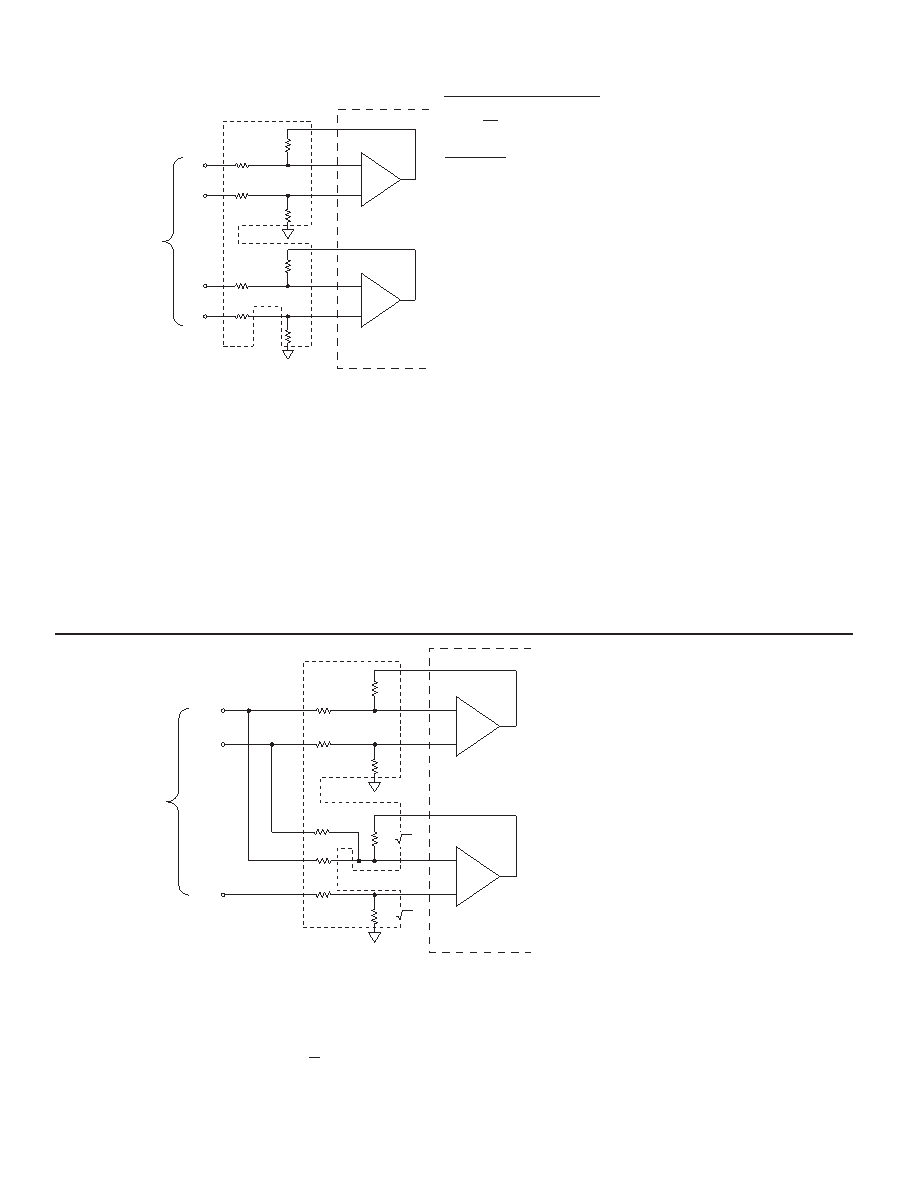
FIGURE 13. DIFFERENTIAL RESOLVER INPUT, USING DDC-49530/57470 (11.8 V) OR DDC-49590 (90 V),
DDC-73089 (2 V) USING DISCRETE RESISTORS
FIGURE 14. SYNCHRO INPUT, USING DDC-49530/57470 (11.8 V), DDC-49590 (90 V)
R i
S1
S3
+S
-S
SIN
R f
R i
R f
R i
S4
S2
+C
-C
R f
R i
R f
COS
A GND
CONVERTER
8 10
12
15
13
2
3
1
6
16
7
4
5
-
+
-
+
RESOLVER
INPUT
See figure 5 for op amp configuration.
S1 and S3, S2 and S4, and RH and RL should be ideally twisted shielded, with the shield tied to GND at the converter.
For DDC-49530: Ri = 70.8 KΩ, 11.8 V input, synchro or resolver.
For DDC-49590: Ri = 270 KΩ, 90 Volt input, synchro or resolver.
Maximum additional error is 1 LSB using recommended thin film packages.
When using discrete resistors: Resolver L-L voltage =
x 2 Vrms, where Rf ≥ 6 kΩ.
For 2V direct input, use 10k
Ω matched resistors for Ri and Rf.
Input options affect DC offset gains and therefore carrier frequency ripple and jitter. Offset gains associated with differential mode
(offset gain for differential configuration = 1+Rf/Ri) and direct mode (offset gain for direct configuration = 1) show differential mode
will always be higher. Higher DC offsets cause higher carrier frequency ripple due to the demodulation process. This carrier frequency
ripple rides on top of the DC error signal, causing jitter. A higher carrier frequency versus bandwidth ratio will help to decrease ripple
and jitter associated with offsets. In summary, R/Ds with differential inputs are more susceptible to offset problems than R/Ds in
single-ended mode. R/Ds in higher resolutions, such as 16 bit, will further compound offset issues due to higher internal voltage
gains. Although the differential configuration has a higher DC offset gain, the differential configuration's common mode noise rejection
makes it the preferred input option. The tradeoffs should be considered on a design to design basis. Also refer to FAQ-GIQ-021.
Ri
Rf
Note: The external BW components
as shown in Figures 1 and 2
are necessary for the R/D to
function.
Examples of Component Calculations:
(1) 2V in, need gain of 1, use 10k for Rf &Ri
Gain = Rf
Ri
(2) 4V in, need gain of 0.5, Ri = 20k, Rf = 10k
To Calculate Ri:
Select 10k for Rf
Ri = Rf x 0.5 (input L-L volt)
Ri = 10k x 0.5 x (L-L volt)
R i
S1
S3
+S
-S
SIN
R f
R i
R f
R i
S2
+C
-C
R /2
i
COS
A GND
CONVERTER
8
15
11
15
14
2
3
1
6
16
7
4
5
R i
9
R / 3
f
R / 3
f
10
-
+
-
+
See figure 5 for op amp configuration.
S1, S2, S3 should be triple twisted shielded; RH and RL should be twisted shielded;
In both cases the shield should be tied to GND at the converter.
11.8 Volt input = DDC-49530: Ri = 70.8 KΩ, 11.8 V input, synchro or resolver.
90 Volt input = DDC-49590: Ri = 270 KΩ, 90 Volt input, synchro or resolver.
Maximum additional error is 1 LSB using recommended thin film package.
When using discrete resistors: Resolver L-L voltage =
x 2 Vrms, where Rf ≥ 6 kΩ
Ri
Rf
SYNCHRO
INPUT
Note: The external BW components
as shown in Figures 1 and 2
are necessary for the R/D to
function.
相关PDF资料 |
PDF描述 |
|---|---|
| RD-19230FX-202T | SYNCHRO OR RESOLVER TO DIGITAL CONVERTER, PQFP64 |
| RD-19240LG200T | SYNCHRO OR RESOLVER TO DIGITAL CONVERTER, PQCC64 |
| RD-19240FSA00T | SYNCHRO OR RESOLVER TO DIGITAL CONVERTER, PQFP52 |
| RD10MWB | 10 V, 0.2 W, SILICON, UNIDIRECTIONAL VOLTAGE REGULATOR DIODE |
| RD15MWB | 15 V, 0.2 W, SILICON, UNIDIRECTIONAL VOLTAGE REGULATOR DIODE |
相关代理商/技术参数 |
参数描述 |
|---|---|
| RD-19230FX-202 | 制造商:未知厂家 制造商全称:未知厂家 功能描述:Resolver-to-Digital Converter |
| RD-19230FX-202T | 制造商:未知厂家 制造商全称:未知厂家 功能描述:Resolver-to-Digital Converter |
| RD-19230FX-203 | 制造商:未知厂家 制造商全称:未知厂家 功能描述:Resolver-to-Digital Converter |
| RD-19230FX-203T | 制造商:未知厂家 制造商全称:未知厂家 功能描述:RESOLVER-TO-DIGITAL CONVERTER |
| RD-19230FX-302 | 制造商:未知厂家 制造商全称:未知厂家 功能描述:Resolver-to-Digital Converter |
发布紧急采购,3分钟左右您将得到回复。