- 您现在的位置:买卖IC网 > PDF目录297235 > RD-19230FX-202T (DATA DEVICE CORP) SYNCHRO OR RESOLVER TO DIGITAL CONVERTER, PQFP64 PDF资料下载
参数资料
| 型号: | RD-19230FX-202T |
| 厂商: | DATA DEVICE CORP |
| 元件分类: | 位置变换器 |
| 英文描述: | SYNCHRO OR RESOLVER TO DIGITAL CONVERTER, PQFP64 |
| 封装: | 0.520 X 0.520 INCH, PLASTIC, QFP-64 |
| 文件页数: | 18/23页 |
| 文件大小: | 476K |
| 代理商: | RD-19230FX-202T |
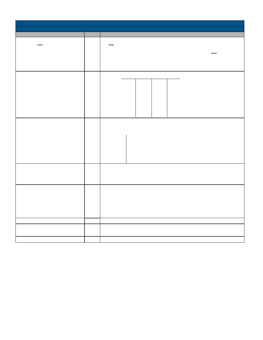
4
Data Device Corporation
www.ddc-web.com
RD-19230
W-05/08-0
TEMPERATURE RANGE
Operating (case)
-30X
-20X
Storage
Junction-to-Case
Junction-to-Ambient
Junction Temp Max
°C
°C/W
°C
0 to +70
-40 to +85
-65 to +150
20
50
150
POWER SUPPLIES
Nominal Voltage
Voltage Range
Max Volt. w/o Damage
Current
V
%
V
mA
(note 6)
+5 (VDD)
-5 (VSS)
±5
+7
-7
25 max. (each), 17 typ.* (* Typical current is when a 30K resistor is used for the current set.)
oz(g)
WEIGHT
0.018 ( 0.5 )
0.52 x 0.52 (13.2 x 13.2)
in(mm)
PHYSICAL
CHARACTERISTICS
Size: 64-pin Quad Flat Pack
DYNAMIC CHARACTERISTICS
Resolution
Tracking Rate (min)
Bandwidth (Closed Loop)
Ka(Acceleration Constant) Note 12
A1
A2
A
B
Acceleration (1 LSB lag)
Settling Time (179° step)
bits
rps
Hz
1/sec2
1/sec
deg/sec2
msec
(at maximum bandwidth)
10
12
14
16
1152
288
72
18
1200
600
300
5.7M
1.4M
360k
19.5
4.9
1.2
295k
2400
1200
600
1200
600
300
2M
500k
30k
2k
2
8
20
50
VELOCITY CHARACTERISTICS
Polarity
Voltage Range (Full Scale) (see note 14)
Scale Factor Error
Scale Factor TC
Reversal Error
Linearity
Zero Offset
Zero Offset TC
Load
V
%
PPM/°C
%
mV
V/°C
k
Ω
Positive for increasing angle
±4 (at nominal power supply)
10 typ
20 max
100 typ
200 max
0.75 typ
1.3 max
0.25 typ
0.50 max
5 typ
10 max
15 typ
30 max
8 min
The BIT error is triggered if any of the following conditions exist: ~ 100 LSB’s of positve error,
~ 250 LSB’s of negative error, Loss of Signal (LOS), or Loss of Reference (LOR) is less than
500 mVp, or a false null occurs when the phase detect circuitry causes a BIT and corrects the
error. Logic 0 for fault condition.
Incremental Encoder Output
TABLE 1. RD-19230 SPECIFICATIONS (CONTINUED)
PARAMETER
UNIT
VALUE
Digital Outputs (cont)
Built-In-Test (BIT)
A, B (see note 14)
These specs apply over the rated power supply, temperature, and reference frequency ranges; 10% signal amplitude variation, and 10% harmonic distortion.
MOISTURE SENSITIVITY LEVEL
Level 2 Tested in accordance with JEDEC SPEC J-STD-020
Notes:
1. As parallel resolution is reduced, pairs of bits are disabled. (Unused bits are set to a logic “0.”)
14 bit resolution: 15/16 disabled, 12 bit resolution: 13/14, 15/16 disabled, 10 bit resolution: 11/12, 13/14, 15/16 disabled
2. In LVDT mode, Bit 3 is the MSB and resolution is programmable to 8, 10, 12, and 14 bits.
3. Accuracy specification below for LVDT mode, null to + full scale travel (45 degrees) (2-wire configuration).
4 Minute part = 0.15% + 1 LSB of full scale “resolution set”
2 Minute part = 0.07% + 1 LSB of full scale “resolution set”
1 Minute part = 0.035% + 1 LSB of full scale “resolution set”
Accuracy specification below for LVDT mode, full scale travel (90 degrees) (3-wire configuration).
4 Minute part = 0.07% + 1 LSB of full scale “resolution set”
2 Minute part = 0.035% + 1 LSB of full scale “resolution set”
1 Minute part = 0.017% + 1 LSB of full scale “resolution set”
Note that these accuracy specifications are for the converter and do not consider any front end external resistor tolerances.
4. In the frequency range of 47Hz to 1kHz, there will be 1 LSB of jitter at quadrant boundaries.
5. The maximum phase shift tolerance will degrade linearly from 45 degrees at 400 Hz to 30 degrees at 60 Hz.
6. When using the -5V inverter, the VDD supply current will double and VSSP can be up to 20% low, or -4V.
7. || = in parallel with.
8. High Z refers to parallel data only.
9. Normal ESD (Electro Static Device) handling precautions should be observed.
10. Any unused pins may be left floating (unconnected). All TTL & CMOS input pins are internally pulled up to +5 Volts.
11. A signal less than 500 mVrms will assert BIT.
12. For Ka definition, see the RD/RDC application manual acceleration lag section.
13. When in overload condition, the converter will not operate to specification and will not be damaged.
14. Dynamic accuracy may be degraded in high bandwidth system applications. See Theory of Operation section for details.
相关PDF资料 |
PDF描述 |
|---|---|
| RD-19240LG200T | SYNCHRO OR RESOLVER TO DIGITAL CONVERTER, PQCC64 |
| RD-19240FSA00T | SYNCHRO OR RESOLVER TO DIGITAL CONVERTER, PQFP52 |
| RD10MWB | 10 V, 0.2 W, SILICON, UNIDIRECTIONAL VOLTAGE REGULATOR DIODE |
| RD15MWB | 15 V, 0.2 W, SILICON, UNIDIRECTIONAL VOLTAGE REGULATOR DIODE |
| RD24MWB | 24 V, 0.2 W, SILICON, UNIDIRECTIONAL VOLTAGE REGULATOR DIODE |
相关代理商/技术参数 |
参数描述 |
|---|---|
| RD-19230FX-203 | 制造商:未知厂家 制造商全称:未知厂家 功能描述:Resolver-to-Digital Converter |
| RD-19230FX-203T | 制造商:未知厂家 制造商全称:未知厂家 功能描述:RESOLVER-TO-DIGITAL CONVERTER |
| RD-19230FX-302 | 制造商:未知厂家 制造商全称:未知厂家 功能描述:Resolver-to-Digital Converter |
| RD-19230FX-302T | 制造商:未知厂家 制造商全称:未知厂家 功能描述:Resolver-to-Digital Converter |
| RD-19230FX-303 | 制造商:未知厂家 制造商全称:未知厂家 功能描述:Resolver-to-Digital Converter |
发布紧急采购,3分钟左右您将得到回复。