- 您现在的位置:买卖IC网 > PDF目录297235 > RD-19240FSA00T (DATA DEVICE CORP) SYNCHRO OR RESOLVER TO DIGITAL CONVERTER, PQFP52 PDF资料下载
参数资料
| 型号: | RD-19240FSA00T |
| 厂商: | DATA DEVICE CORP |
| 元件分类: | 位置变换器 |
| 英文描述: | SYNCHRO OR RESOLVER TO DIGITAL CONVERTER, PQFP52 |
| 封装: | PLASTIC, MQFP-52 |
| 文件页数: | 17/18页 |
| 文件大小: | 215K |
| 代理商: | RD-19240FSA00T |
8
Data Device Corporation
www.ddc-web.com
RD-19240
Pre 1-1-04/05-0
+S
-S
SIN
aR
R
+C
-C
COS
R
-
+
-
+
R
aR
C1
bR
2R
R
bR
+REF
-REF
R
C2
2 WIRE LVDT
REF IN
R
2 V
FS = 2 V
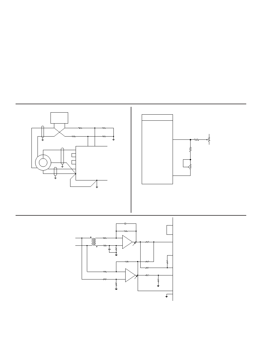
FIGURE 8. 2-WIRE LVDT DIRECT INPUT
C1 = C2, set for phase lag = phase lead through the LVDT.
LVDT (LINEAR VARIABLE DIFFERENTIAL
TRANSFORMER) MODE
As shown in TABLE 1 the RD-19240 unit can be made to operate
as a LVDT-to-digital converter by connecting Resolution Control
inputs A and B to “0”, “1”, or the -5 volt supply. In this mode the
RD-19240 functions as a ratiometric tracking linear converter.
When linear AC inputs are applied from an LVDT the converter
operates over one quarter of its range. This results in two less bits
of resolution for LVDT mode than are provided in resolver mode.
The LVDT output signals will need to be scaled to be compatible
with the converter input. FIGURE 9 is a schematic of an input
scaling circuit applicable to 3-wire LVDTs. The value of the scal-
ing constant “a” is selected to provide an input of 2 Vrms at full
stroke of the LVDT. The value of scaling constant “b” is selected to
provide an input of 1 Vrms at null of the LVDT. Suggested com-
ponents for implementing the input scaling circuit are a quad op-
amp, such as a 4741 type, and precision thin-film resistors of
0.1% tolerance. FIGURE 8 illustrates a 2-wire LVDT configuration.
Data output of the RD-19240 is Binary Coded in LVDT mode. The
most negative stroke of the LVDT is represented by ALL ZEROS
and the most positive stroke of the LVDT is represented by ALL
ONES. The most significant 2 bits (2 MSBs) may be used as
overrange indicators. Positive overrange is indicated by code “01”
and negative overrange is indicated by code “11” (see TABLE 5).
R1
R 3
R 2
R 4
EXTERNAL
REF
LO
HI
RESOLVER
S4
S3
S1
S2
GND
+S
-S
SIN
COS
-C
+C
A GND
-R
+R
Notes:
1) Resistors selected to limit Vref peak to between 1.5 V and 5 V.
2) If external reference LO is grounded, then R3 and R4 are not
needed, and -R is connected to GND.
3) 10k ohms, 1 % series current limit resistors are recommended.
See Note 3.
Note: Five external BW components
as shown in Figures 1 and 2
are necessary for the R/D to
function.
FIGURE 6. TYPICAL CONNECTIONS, 2 VOLT
RESOLVER, DIRECT INPUT
2
1
-VCO
VEL
+5 V
-5 V
100 k
(OFFSET)
100 RV
0.8 RV
0.4 R (SCALING)
V
RD-19240
FIGURE 7. VELOCITY TRIMMING
相关PDF资料 |
PDF描述 |
|---|---|
| RD10MWB | 10 V, 0.2 W, SILICON, UNIDIRECTIONAL VOLTAGE REGULATOR DIODE |
| RD15MWB | 15 V, 0.2 W, SILICON, UNIDIRECTIONAL VOLTAGE REGULATOR DIODE |
| RD24MWB | 24 V, 0.2 W, SILICON, UNIDIRECTIONAL VOLTAGE REGULATOR DIODE |
| RD27MWB | 27 V, 0.2 W, SILICON, UNIDIRECTIONAL VOLTAGE REGULATOR DIODE |
| RD9.1MWB | 9.1 V, 0.2 W, SILICON, UNIDIRECTIONAL VOLTAGE REGULATOR DIODE |
相关代理商/技术参数 |
参数描述 |
|---|---|
| RD1-9320 | 制造商:STMicroelectronics 功能描述:MPU DEMO-BOARD |
| RD1950MPXM2010GS | 制造商:Freescale Semiconductor 功能描述:WATER LEVEL REFERENCE DESIGN - Bulk |
| RD1986MMA2260D | 功能描述:加速传感器开发工具 TRIAX REF DSGN 3-AXIS FOR MMA2260D RoHS:否 制造商:Murata 工具用于评估:SCA3100-D04 加速:2 g 传感轴:Triple Axis 接口类型:SPI 工作电压:3.3 V |
| RD1986MMA6260Q | 功能描述:加速传感器开发工具 TRIAX REF DSGN 3-AXIS FOR NMA6260Q RoHS:否 制造商:Murata 工具用于评估:SCA3100-D04 加速:2 g 传感轴:Triple Axis 接口类型:SPI 工作电压:3.3 V |
| RD1A-12S | 制造商:World Products 功能描述: |
发布紧急采购,3分钟左右您将得到回复。