- 您现在的位置:买卖IC网 > PDF目录297235 > RD-19240LG200T (DATA DEVICE CORP) SYNCHRO OR RESOLVER TO DIGITAL CONVERTER, PQCC64 PDF资料下载
参数资料
| 型号: | RD-19240LG200T |
| 厂商: | DATA DEVICE CORP |
| 元件分类: | 位置变换器 |
| 英文描述: | SYNCHRO OR RESOLVER TO DIGITAL CONVERTER, PQCC64 |
| 封装: | PLASTIC, LCC-64 |
| 文件页数: | 4/18页 |
| 文件大小: | 215K |
| 代理商: | RD-19240LG200T |
12
Data Device Corporation
www.ddc-web.com
RD-19240
Pre 1-1-04/05-0
ponents to settle to the pre-charged level. This time will
depend on the time constant of the bandwidth components
being charged. If switching is limited to two adjacent resolu-
tions (i.e., 12 and 14) then the pre-charge amplifier can be set
up to continuously maintain the appropriate velocity voltage
on the deselected components, resulting in the fastest possi-
ble switching times. See FIGURE 13 for an example of the
input wiring connections necessary for switching-on-the-fly
between 10 and 12 bit resolution.
DUAL BANDWIDTHS
With the second set of BW component pads, the user can set
two bandwidths for the RD-19240 and choose between them. To
use two bandwidths, proceed as follows:
1) Tie UP/DN to pad -5V.
2) Choose the two bandwidths following the guidelines in the
General Setup Considerations; the RV resistor must be the
same value for both bandwidths.
3) Use the SHIFT pad to choose between bandwidths. A logic 1
selects the VEL1 components and a logic 0 selects the VEL2
components.
INTERNAL ENCODER EMULATION
The RD-19240 can be programmed to encoder emulation mode
by toggling the A_QUAD_B input to a logic 0. The U/B output pad
becomes B (LSB XOR LSB + 1). The A (LSB + 1) and B output
signals can be used in control systems that are designed to inter-
face with incremental optical encoders. To enable the Zero Index
pulse, ZIP_EN should be tied to a logic 0.
An example circuit to create a low going edge of A_QUAD_B is
depicted in FIGURE 18. If the power supply takes longer than
50ms to start up then the time constant of 50ms set in FIGURE
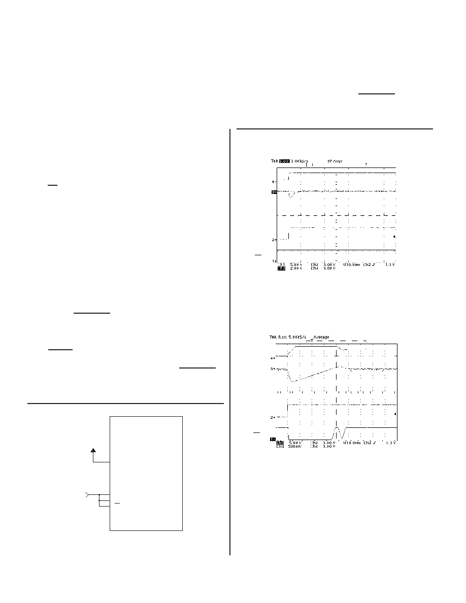
FIGURE 14. BENEFIT OF SWITCHING
RESOLUTION ON THE FLY
Without Switch Resolution on the Fly Implemented
With Switch Resolution on the Fly Implemented
GND
UP/DN
SHIFT
RD-19240
D1
D0
CONTROL
FIGURE 13. INPUT WIRING - SWITCHING-ON-THE-
FLY BETWEEN 12- AND 14-BIT RESOLUTION
VEL
0V
-5V
ERROR 0
D0
0V
5V
BIT
0V
5V
ERROR = 13.6 LSBs per box
Note: Depending on bandwidth, step error may be greater.
VEL
0V
-5V
ERROR 0
D0
0V
5V
BIT
0V
5V
ERROR = 1500 LSBs per box
18 will require being extended. Alternatively a system logic reset
signal or internally generated logic ‘load’ pulse can be generated
to latch in the encoder resolution.
The resolution of the incremental outputs is latched from the D0
and D1 inputs on the low going edge of A_QUAD_B. The resolu-
tion of the parallel data outputs may be changed any time after
the encoder resolution is latched (see FIGURE 17).
Note: Depending on bandwidth, step error may be greater.
Also, less velocity / movement will lessen the error
glitch shown in the graph. The graph shows a worst
case condition based upon one bandwidth and track-
ing rate set-up. Worst case is when the overshoot on
the velocity hits the saturation point as per the graph.
相关PDF资料 |
PDF描述 |
|---|---|
| RD-19240FSA00T | SYNCHRO OR RESOLVER TO DIGITAL CONVERTER, PQFP52 |
| RD10MWB | 10 V, 0.2 W, SILICON, UNIDIRECTIONAL VOLTAGE REGULATOR DIODE |
| RD15MWB | 15 V, 0.2 W, SILICON, UNIDIRECTIONAL VOLTAGE REGULATOR DIODE |
| RD24MWB | 24 V, 0.2 W, SILICON, UNIDIRECTIONAL VOLTAGE REGULATOR DIODE |
| RD27MWB | 27 V, 0.2 W, SILICON, UNIDIRECTIONAL VOLTAGE REGULATOR DIODE |
相关代理商/技术参数 |
参数描述 |
|---|---|
| RD1-9320 | 制造商:STMicroelectronics 功能描述:MPU DEMO-BOARD |
| RD1950MPXM2010GS | 制造商:Freescale Semiconductor 功能描述:WATER LEVEL REFERENCE DESIGN - Bulk |
| RD1986MMA2260D | 功能描述:加速传感器开发工具 TRIAX REF DSGN 3-AXIS FOR MMA2260D RoHS:否 制造商:Murata 工具用于评估:SCA3100-D04 加速:2 g 传感轴:Triple Axis 接口类型:SPI 工作电压:3.3 V |
| RD1986MMA6260Q | 功能描述:加速传感器开发工具 TRIAX REF DSGN 3-AXIS FOR NMA6260Q RoHS:否 制造商:Murata 工具用于评估:SCA3100-D04 加速:2 g 传感轴:Triple Axis 接口类型:SPI 工作电压:3.3 V |
| RD1A-12S | 制造商:World Products 功能描述: |
发布紧急采购,3分钟左右您将得到回复。