- 您现在的位置:买卖IC网 > PDF目录376305 > REJ03C0098_R1LV0408C (Hitachi,Ltd.) Wide Temperature Range Version 4M SRAM (512-kword 】 8-bit) PDF资料下载
参数资料
| 型号: | REJ03C0098_R1LV0408C |
| 厂商: | Hitachi,Ltd. |
| 英文描述: | Wide Temperature Range Version 4M SRAM (512-kword 】 8-bit) |
| 中文描述: | 宽温版本4分的SRAM(512 - KWord的】8位) |
| 文件页数: | 8/14页 |
| 文件大小: | 94K |
| 代理商: | REJ03C0098_R1LV0408C |
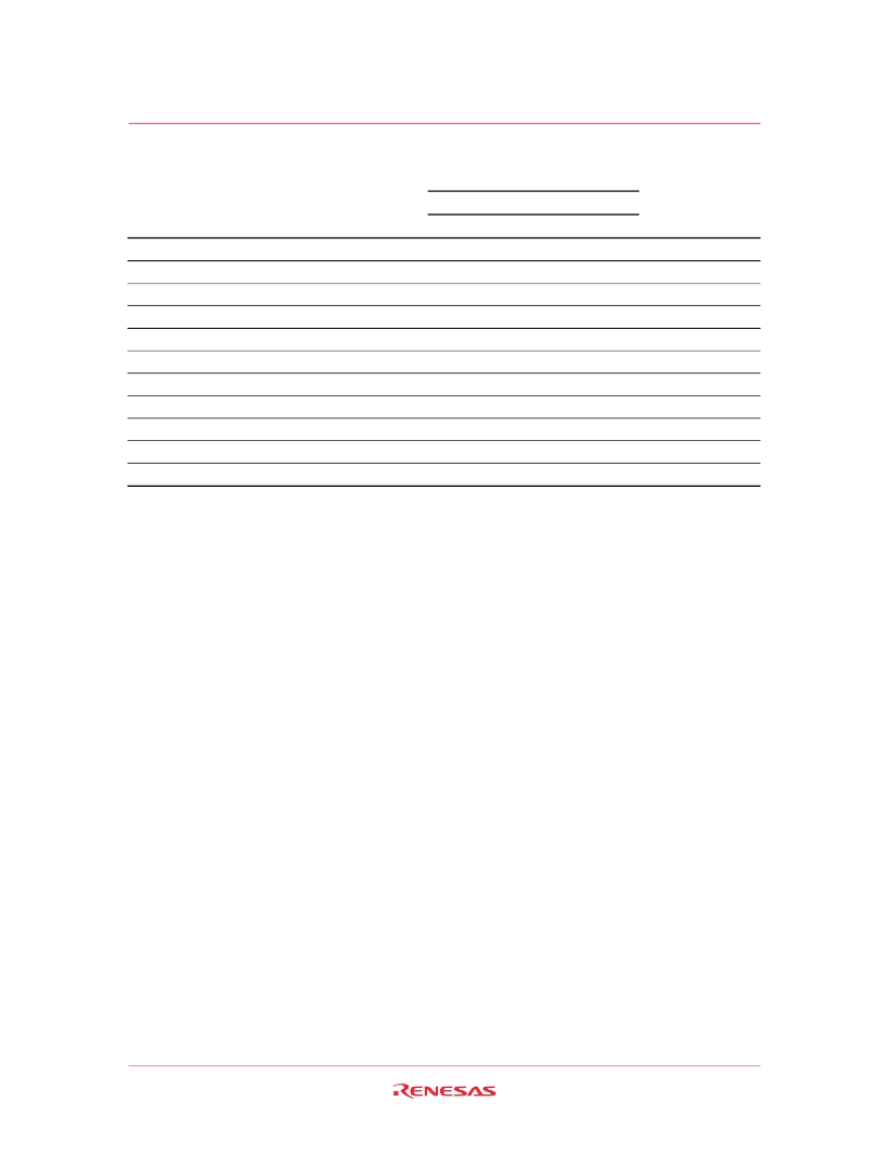
R1LV0408C-I Series
Rev.2.00, May.25.2004, page 8 of 12
Write Cycle
R1LV0408C-I
-5SI
-7LI
Parameter
Symbol
Min
Max
Min
Max
Unit
Notes
Write cycle time
t
WC
t
CW
t
AS
t
AW
t
WP
t
WR
t
WHZ
t
DW
t
DH
t
OW
t
OHZ
55
20
20
70
25
25
ns
Chip selection to end of write
50
60
ns
4
Address setup time
0
0
ns
5
Address valid to end of write
50
60
ns
Write pulse width
40
50
ns
3, 12
Write recovery time
0
0
ns
6
Write to output in high-Z
0
0
ns
1, 2, 7
Data to write time overlap
25
30
ns
Data hold from write time
0
0
ns
Output active from end of write
5
5
ns
2
Output disable to output in high-Z
Notes: 1. t
HZ
, t
OHZ
and t
WHZ
are defined as the time at which the outputs achieve the open circuit conditions
and are not referred to output voltage levels.
2. This parameter is sampled and not 100% tested.
3. A write occurs during the overlap (t
WP
) of a low CS# and a low WE#. A write begins at the later
transition of CS# going low or WE# going low. A write ends at the earlier transition of CS# going
high or WE# going high. t
WP
is measured from the beginning of write to the end of write.
4. t
CW
is measured from CS# going low to the end of write.
5. t
AS
is measured from the address valid to the beginning of write.
6. t
WR
is measured from the earlier of WE# or CS# going high to the end of write cycle.
7. During this period, I/O pins are in the output state so that the input signals of the opposite phase
to the outputs must not be applied.
8. If the CS# low transition occurs simultaneously with the WE# low transition or after the WE#
transition, the output remain in a high impedance state.
9. Dout is the same phase of the write data of this write cycle.
10. Dout is the read data of next address.
11. If CS# is low during this period, I/O pins are in the output state. Therefore, the input signals of
the opposite phase to the outputs must not be applied to them.
12. In the write cycle with OE# low fixed, t
WP
must satisfy the following equation to avoid a problem of
data bus contention. t
WP
≥
t
DW
min + t
WHZ
max
0
0
ns
1, 2, 7
相关PDF资料 |
PDF描述 |
|---|---|
| REJ03F0010_M61529FP | LEAD FREE EXT TEMP A6832 PLCC |
| REJ03F0023_M61140FP | TUNER SINGLE CHIP |
| REJ03F0035_M61524FP | 2ch ELECTRONIC VOLUME WITH 4 INPUT SELECTOR |
| REJ03F0040_M61528FP | LEAD FREE A6832 PLCC |
| REJ03F0041_M61532FP | 8ch Electronic Volume with 9 Input Selector |
相关代理商/技术参数 |
参数描述 |
|---|---|
| REJ03C0115-0100Z | 制造商:RENESAS 制造商全称:Renesas Technology Corp 功能描述:4M HIGH SPEED SRAM (1-MWORD X 4-BIT) |
| REJ03F0010_M61529FP | 制造商:HITACHI 制造商全称:Hitachi Semiconductor 功能描述:Audio Signal Processor with Surround |
| REJ03F0023_M61140FP | 制造商:HITACHI 制造商全称:Hitachi Semiconductor 功能描述:TUNER SINGLE CHIP |
| REJ03F0034_M61522FP | 制造商:未知厂家 制造商全称:未知厂家 功能描述:8ch ELECTRONIC VOLUME WITH 8 INPUT SELECTOR |
| REJ03F0035_M61524FP | 制造商:HITACHI 制造商全称:Hitachi Semiconductor 功能描述:2ch ELECTRONIC VOLUME WITH 4 INPUT SELECTOR |
发布紧急采购,3分钟左右您将得到回复。