- 您现在的位置:买卖IC网 > PDF目录96803 > S1C33L05 RISC MICROCONTROLLER, PQFP176 PDF资料下载
参数资料
| 型号: | S1C33L05 |
| 元件分类: | 微控制器/微处理器 |
| 英文描述: | RISC MICROCONTROLLER, PQFP176 |
| 封装: | 24 X 24 MM, 1.40 MM HEIGHT, 0.50 MM PITCH, PLASTIC, QFP21-176 |
| 文件页数: | 7/8页 |
| 文件大小: | 81K |
| 代理商: | S1C33L05 |
7
S1C33L05
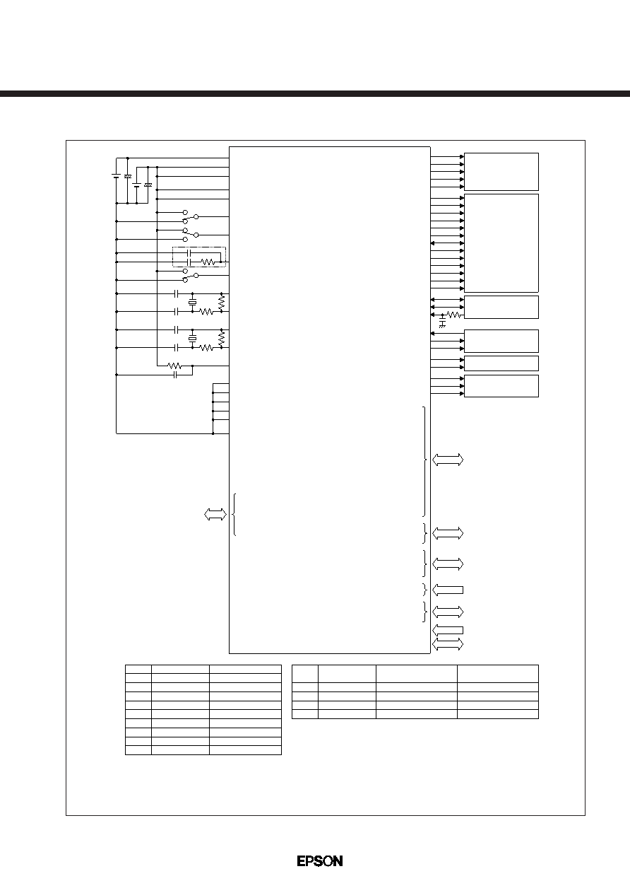
■ BASIC EXTERNAL CONNECTION DIAGRAM
Fig. 3 Basic External Connection Diagram
X'tal1
CG1
CD1
Rf1
Rd1
R1
C1
C2
R2
C3
Crystal resonator
Gate capacitor
Drain capacitor
Feedback resistor
Drain resistor
Resistor
Capacitor
Resistor
Capacitor
32.768 kHz
12 pF
10 M
0
4.7 k
100 pF
3 pF
10
1
F
X'tal2
or CE
CG2
CD2
Rf2
Rd2
Resonator
Gate capacitor
Drain capacitor
Feedback resistor
Drain resistor
Crystal
3 pF
4 pF
1 M
0
Ceramic
(CSTCW48M0X11
)
(6 pF)
22 k
47
Note:
1Oscillation characteristics vary depending on conditions (components
used, board pattern, etc.). The values in the above table are shown only
for reference and not guaranteed. In particular, ceramic oscillation is
extremely sensitive to influence of external components and printed-
circuit boards. Before using a ceramic resonator, please be sure to
contact Murata Manufacturing Co., Ltd. for further information on
conditions of use for ceramic resonators. Furthermore, this chip supports
only 48-MHz ceramic resonators. Do not use ceramic resonators with
any other frequency.
2 Capacitance built into the ceramic resonator
S1C33L05
[The potential of the substrate
(back of the chip) is VSS.]
External
Bus
HSDMA
Serial I/O
A/D input
Input
I/O
Timer
input/output
1: When the PLL is not used,
leave the PLLC pin open.
FPFRAME
FPLINE
FPDAT[7:0]([7:4])
FPSHIFT
DRDY
SDCLK
SDCKE
A[15:14]
A12
SDA10
A[10:1]
D[15:0]
UDQM
LDQM
#SDCE
#SDRAS
#SDCAS
#SDWE
USBDP
USBDM
USBVBUS
SDI
SDO
SPICLK
#SMWE
#SMRE
SQLALE
SQUALE
#SQRD
A[25:1], A0/#BSL
D[15:0]
#RD
#GARD
#GAAS
#WRL/#WR
#WRH/#BSH
#CExx
#CE10EX
#WAIT
BCLK
#BUSREQ
#BUSACK
#BUSGET
#NMI
#DMAREQx
#DMAACKx
#DMAENDx
SINx/FSIN0
SOUTx/FSOUT0
#SCLKx/#FSCLK0
#SRDYx/#FSRDY0
#ADTRG
ADx
EXCLx
TMx
T8UFx
Kxx
Pxx
LCD
USB
(host)
NAND flash
MMC
Debug
interface
VDD
VDDE
AVDDE
EA10MD0
EA10MD1
#X2SPD
BOOT
PLLC
PLLS0
OSC3
OSC4
OSC1
OSC2
#RESET
TST
TEST1
TEST2
SCANEN
BURNIN
VSS
FOSC1
DST[2:0]
DPCO
DCLK
DSIO
1.8 V
3.3 V
Rd2
Rd1
CD2
X'tal2 or CE
Rf2
CG2
CD1
X'tal1
Rf1
CG1
C2
C1
R1
1
+
DP
DM
VBUS
DI
DO
CLK, CS
#WE
#RE
SQ ROM
ALEL
ALEH
#RD
YD
LP
XD[7:0]([7:4])
XSCL
FR
SDRAM
(4M x 16)
CLK
CKE
BA[1:0]
A11
A10
A[9:0]
DQ[15:0]
DQMH
DQML
#CS
#RAS
#CAS
#WE
C3
R2
1, 2
1
相关PDF资料 |
PDF描述 |
|---|---|
| S1C33S01F00A300 | 32-BIT, 50 MHz, RISC MICROCONTROLLER, PQFP100 |
| S1C33T01F00A200 | 32-BIT, 60 MHz, RISC MICROCONTROLLER, PQFP176 |
| S1R72803F00A | 1 CHANNEL(S), 400M bps, SERIAL COMM CONTROLLER, PQFP184 |
| S2164 | PHOTO DIODE |
| S21MD3VI | 1 CHANNEL TRIAC OUTPUT OPTOCOUPLER |
相关代理商/技术参数 |
参数描述 |
|---|---|
| S1C33L11 | 制造商:EPSON 制造商全称:EPSON 功能描述:32-bit Single Chip Microcomputer |
| S1C33L15 | 制造商:EPSON 制造商全称:EPSON 功能描述:CMOS 32-bit Application Specific Controller |
| S1C33L17 | 制造商:EPSON 制造商全称:EPSON 功能描述:CMOS 32-bit Application Specific Controller |
| S1C33L17D00A000 | 制造商:Seiko Instruments Inc (SII) 功能描述:IC 32BIT MCU 33L17 DIE FORM |
| S1C33L19 | 制造商:EPSON 制造商全称:EPSON 功能描述:CMOS 32-bit application Specific Controller |
发布紧急采购,3分钟左右您将得到回复。