- 您现在的位置:买卖IC网 > PDF目录225140 > S29GL032A11BFIR31 (Spansion Inc.) 64 MEGABIT 32MEGABIT 3.0 BOLT ONLY PAGE MODE FLASH MEMORY PDF资料下载
参数资料
| 型号: | S29GL032A11BFIR31 |
| 厂商: | Spansion Inc. |
| 英文描述: | 64 MEGABIT 32MEGABIT 3.0 BOLT ONLY PAGE MODE FLASH MEMORY |
| 中文描述: | 64兆位32MEGABIT 3.0螺栓只页面模式闪存 |
| 文件页数: | 54/88页 |
| 文件大小: | 1425K |
| 代理商: | S29GL032A11BFIR31 |
第1页第2页第3页第4页第5页第6页第7页第8页第9页第10页第11页第12页第13页第14页第15页第16页第17页第18页第19页第20页第21页第22页第23页第24页第25页第26页第27页第28页第29页第30页第31页第32页第33页第34页第35页第36页第37页第38页第39页第40页第41页第42页第43页第44页第45页第46页第47页第48页第49页第50页第51页第52页第53页当前第54页第55页第56页第57页第58页第59页第60页第61页第62页第63页第64页第65页第66页第67页第68页第69页第70页第71页第72页第73页第74页第75页第76页第77页第78页第79页第80页第81页第82页第83页第84页第85页第86页第87页第88页
56
S29GLxxxA MirrorBit Flash Family
S29GLxxxA_00_A2 January 28, 2005
Ad van c e
Inf o rmation
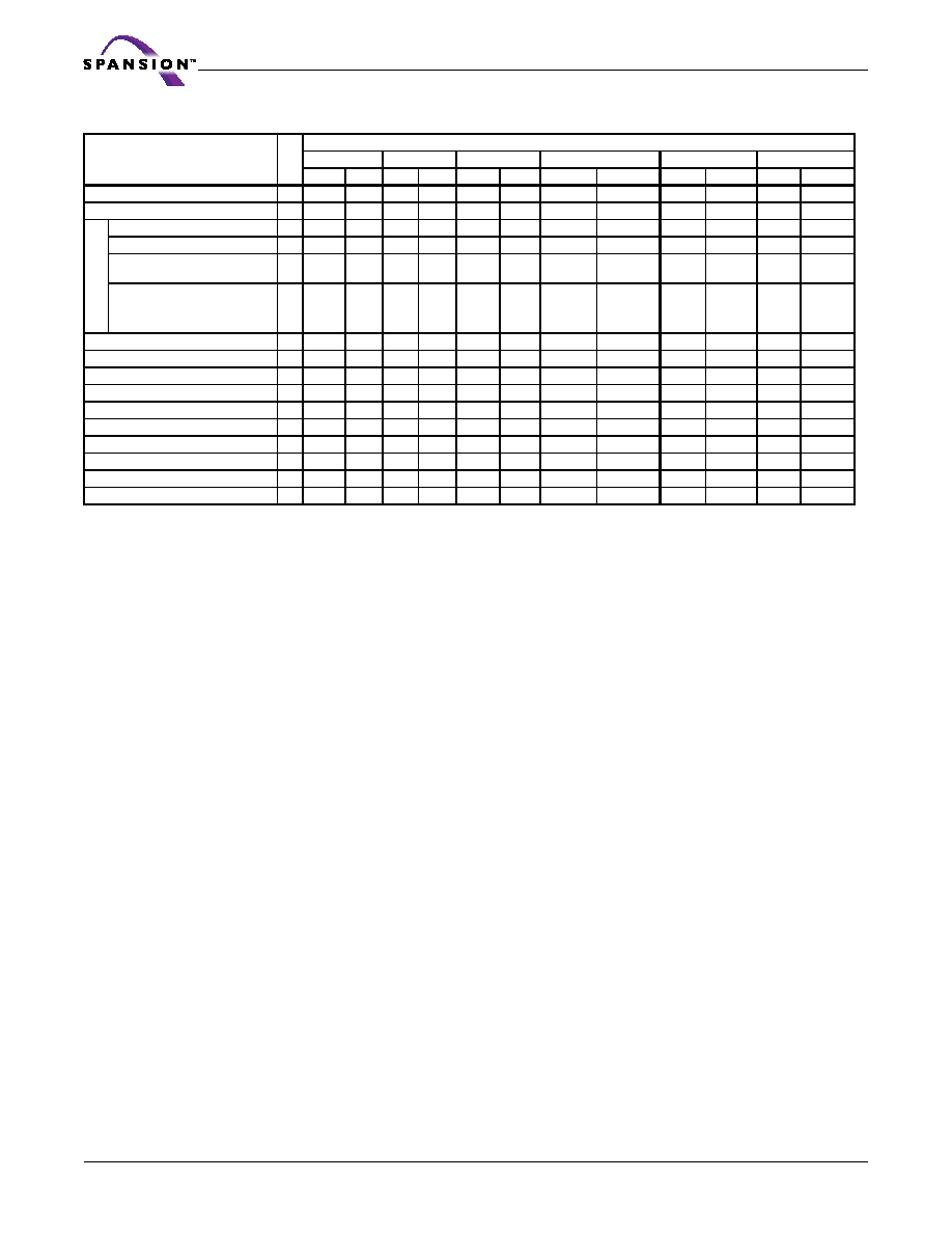
Table 26. Command Definitions (x8 Mode, BYTE# = VIL)
Command
Sequence
(Note 1)
Cyc
le
s
Bus Cycles (Notes 2–5)
First
Second
Third
Fourth
Fifth
Sixth
Addr Data Addr Data Addr Data
Addr
Data
Addr
Data
Addr
Data
Read (Note 6)
1
RA
RD
Reset (Note 7)
1
XXX
F0
A
u
tose
le
ct
(Note
8)
Manufacturer ID
4
AAA
AA
555
55
AAA
90
X00
01
Device ID (Note 9)
4
AAA
AA
555
55
AAA
90
X02
7E
X1C
X1E
Secured Silicon Sector Factory
Protect (Note 10)
4
AAA
AA
555
55
AAA
90
X06
(Note 10)
Sector Group Protect Verify (Note
4
AAA
AA
555
55
AAA
90
(SA)X04
00/01
Enter Secured Silicon Sector Region
3
AAA
AA
555
55
AAA
88
Exit Secured Silicon Sector Region
4
AAA
AA
555
55
AAA
90
XXX
00
Write to Buffer (Note 11)
3
AAA
AA
555
55
SA
25
SA
BC
PA
PD
WBL
PD
Program Buffer to Flash
1
SA
29
Write to Buffer Abort Reset (Note 13)
3
AAA
AA
555
55
AAA
F0
Chip Erase
6
AAA
AA
555
55
AAA
80
AAA
AA
555
55
AAA
10
Sector Erase
6
AAA
AA
555
55
AAA
80
AAA
AA
555
55
SA
30
Program/Erase Suspend (Note 14)
1
XXX
B0
Program/Erase Resume (Note 15)
1
XXX
30
CFI Query (Note 16)
1
AA
98
Legend:
X = Don’t care
RA = Read Address of memory location to be read.
RD = Read Data read from location RA during read operation.
PA = Program Address. Addresses latch on falling edge of WE# or
CE# pulse, whichever happens later.
PD = Program Data for location PA. Data latches on rising edge of
WE# or CE# pulse, whichever happens first.
SA = Sector Address of sector to be verified (in autoselect mode) or
erased. Address bits A21–A15 uniquely select any sector.
WBL = Write Buffer Location. Address must be within same write
buffer page as PA.
BC = Byte Count. Number of write buffer locations to load minus 1.
Notes:
1. See Table 3 for description of bus operations.
2. All values are in hexadecimal.
3. Shaded cells indicate read cycles. All others are write cycles.
4. During unlock and command cycles, when lower address bits are
555 or AAA as shown in table, address bits above A11 are don’t
care.
5. Unless otherwise noted, address bits A21–A11 are don’t cares.
6. No unlock or command cycles required when device is in read
mode.
7. Reset command is required to return to read mode (or to erase-
suspend-read mode if previously in Erase Suspend) when device
is in autoselect mode, or if DQ5 goes high while device is
providing status information.
8. Fourth cycle of autoselect command sequence is a read cycle.
Data bits DQ15–DQ8 are don’t care. See Autoselect Command
Sequence section or more information.
9. Device ID must be read in three cycles.
10. If WP# protects highest address sector, data is 98h for factory
locked and 18h for not factory locked. If WP# protects lowest
address sector, data is 88h for factory locked and 08h for not
factor locked.
11. Data is 00h for an unprotected sector group and 01h for a
protected sector group.
12. Total number of cycles in command sequence is determined by
number of bytes written to write buffer. Maximum number of
cycles in command sequence is 37, including “Program Buffer to
Flash” command.
13. Command sequence resets device for next command after
aborted write-to-buffer operation.
14. System may read and program in non-erasing sectors, or enter
autoselect mode, when in Erase Suspend mode. Erase Suspend
command is valid only during a sector erase operation.
15. Erase Resume command is valid only during Erase Suspend
mode.
16. Command is valid when device is ready to read array data or
when device is in autoselect mode.
17. Refer to Table 12, AutoSelect Codes for individual Device IDs
per device density and model number.
相关PDF资料 |
PDF描述 |
|---|---|
| S29GL032A11BFIR41 | 64 MEGABIT 32MEGABIT 3.0 BOLT ONLY PAGE MODE FLASH MEMORY |
| S29GL032A90TAIR21 | 64 MEGABIT 32MEGABIT 3.0 BOLT ONLY PAGE MODE FLASH MEMORY |
| S29GL032A90TAIR31 | 64 MEGABIT 32MEGABIT 3.0 BOLT ONLY PAGE MODE FLASH MEMORY |
| S29GL032M10BAIR50 | MirrorBit Flash Family |
| S29GL032M10BAIR52 | MirrorBit Flash Family |
相关代理商/技术参数 |
参数描述 |
|---|---|
| S29GL032A11BFIR32 | 制造商:SPANSION 制造商全称:SPANSION 功能描述:64 MEGABIT 32MEGABIT 3.0 BOLT ONLY PAGE MODE FLASH MEMORY |
| S29GL032A11BFIR33 | 制造商:SPANSION 制造商全称:SPANSION 功能描述:64 MEGABIT 32MEGABIT 3.0 BOLT ONLY PAGE MODE FLASH MEMORY |
| S29GL032A11BFIR40 | 制造商:Spansion 功能描述: 制造商:Spansion 功能描述:Flash - NOR IC |
| S29GL032A11BFIR41 | 制造商:SPANSION 制造商全称:SPANSION 功能描述:64 MEGABIT 32MEGABIT 3.0 BOLT ONLY PAGE MODE FLASH MEMORY |
| S29GL032A11BFIR42 | 制造商:SPANSION 制造商全称:SPANSION 功能描述:64 MEGABIT 32MEGABIT 3.0 BOLT ONLY PAGE MODE FLASH MEMORY |
发布紧急采购,3分钟左右您将得到回复。