- 您现在的位置:买卖IC网 > PDF目录98071 > S80C186XL20 (INTEL CORP) 16-BIT, 20 MHz, MICROPROCESSOR, PQFP80 PDF资料下载
参数资料
| 型号: | S80C186XL20 |
| 厂商: | INTEL CORP |
| 元件分类: | 微控制器/微处理器 |
| 英文描述: | 16-BIT, 20 MHz, MICROPROCESSOR, PQFP80 |
| 封装: | EIAJ, QFP-80 |
| 文件页数: | 44/48页 |
| 文件大小: | 762K |
| 代理商: | S80C186XL20 |
第1页第2页第3页第4页第5页第6页第7页第8页第9页第10页第11页第12页第13页第14页第15页第16页第17页第18页第19页第20页第21页第22页第23页第24页第25页第26页第27页第28页第29页第30页第31页第32页第33页第34页第35页第36页第37页第38页第39页第40页第41页第42页第43页当前第44页第45页第46页第47页第48页
80C186XL80C188XL
Bus Interface Unit
The 80C186XL provides a local bus controller to
generate the local bus control signals In addition it
employs a HOLDHLDA protocol for relinquishing
the local bus to other bus masters It also provides
outputs that can be used to enable external buffers
and to direct the flow of data on and off the local
bus
The bus controller is responsible for generating 20
bits of address read and write strobes bus cycle
status information and data (for write operations) in-
formation It is also responsible for reading data
from the local bus during a read operation Synchro-
nous and asynchronous ready input pins are provid-
ed to extend a bus cycle beyond the minimum four
states (clocks)
The 80C186XL bus controller also generates two
control signals (DEN and DTR) when interfacing to
external transceiver chips This capability allows the
addition of transceivers for simple buffering of the
multiplexed addressdata bus
During RESET the local bus controller will perform
the following action
Drive DEN RD and WR HIGH for one clock cy-
cle then float them
Drive S0–S2 to the inactive state (all HIGH) and
then float
Drive LOCK HIGH and then float
Float AD0–15 (AD0–8) A16–19 (A9–A19) BHE
(RFSH) DTR
Drive ALE LOW
Drive HLDA LOW
RD QSMD
UCS
LCS
MCS0 PEREQ
MCS1
ERROR and TEST BUSY pins have internal pullup
devices which are active while RES is applied Ex-
cessive loading or grounding certain of these pins
causes the 80C186XL to enter an alternative mode
of operation
RD QSMD low results in Queue Status Mode
UCS and LCS low results in ONCE Mode
TEST BUSY low (and high later) results in En-
hanced Mode
80C186XL PERIPHERAL
ARCHITECTURE
All the 80C186XL integrated peripherals are con-
trolled by 16-bit registers contained within an inter-
nal 256-byte control block The control block may be
mapped into either memory or IO space Internal
logic will recognize control block addresses and re-
spond to bus cycles An offset map of the 256-byte
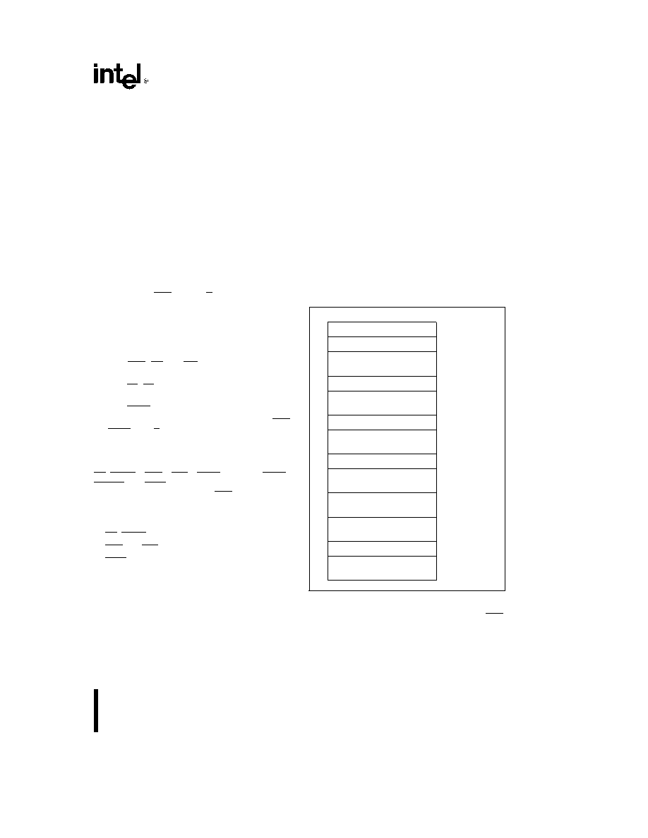
control register block is shown in Figure 3
Chip-SelectReady Generation Logic
The 80C186XL contains logic which provides
programmable chip-select generation for both mem-
ories and peripherals
In addition
it can be
programmed to provide READY (or WAIT state) gen-
eration It can also provide latched address bits A1
and A2 The chip-select lines are active for all mem-
ory and IO cycles in their programmed areas
whether they be generated by the CPU or by the
integrated DMA unit
The 80C186XL provides 6 memory chip select out-
puts for 3 address areas upper memory lower
memory and midrange memory One each is provid-
ed for upper memory and lower memory while four
are provided for midrange memory
OFFSET
Relocation Register
FEH
DMA Descriptors Channel 1
DAH
D0H
DMA Descriptors Channel 0
CAH
C0H
Chip-Select Control Registers
A8H
A0H
Time 2 Control Registers
66H
60H
Time 1 Control Registers
5EH
58H
Time 0 Control Registers
56H
50H
Interrupt Controller Registers
3EH
20H
Figure 3 Internal Register Map
The 80C186XL provides a chip select called UCS
for the top of memory The top of memory is usually
used as the system memory because after reset the
80C186XL begins executing at memory location
FFFF0H
5
相关PDF资料 |
PDF描述 |
|---|---|
| S80C188XL20 | 16-BIT, 20 MHz, MICROPROCESSOR, PQFP80 |
| S80C188XL12 | 16-BIT, 12 MHz, MICROPROCESSOR, PQFP80 |
| SB80C186XL25 | 16-BIT, 25 MHz, MICROPROCESSOR, PQFP80 |
| SB80C188XL25 | 16-BIT, 25 MHz, MICROPROCESSOR, PQFP80 |
| S80C188EB-8 | 8-BIT, 8 MHz, MICROPROCESSOR, PQFP80 |
相关代理商/技术参数 |
参数描述 |
|---|---|
| S80C186XL25 | 功能描述:IC MPU 16-BIT 5V 25MHZ 80-MQFP RoHS:否 类别:集成电路 (IC) >> 嵌入式 - 微处理器 系列:- 标准包装:2 系列:MPC8xx 处理器类型:32-位 MPC8xx PowerQUICC 特点:- 速度:133MHz 电压:3.3V 安装类型:表面贴装 封装/外壳:357-BBGA 供应商设备封装:357-PBGA(25x25) 包装:托盘 |
| S80C188 | 制造商:AMD 制造商全称:Advanced Micro Devices 功能描述:CMOS High-Integration 16-Bit Microprocessors |
| S80C188-12 | 制造商:AMD 制造商全称:Advanced Micro Devices 功能描述:CMOS High-Integration 16-Bit Microprocessors |
| S80C188-16 | 制造商:AMD 制造商全称:Advanced Micro Devices 功能描述:CMOS High-Integration 16-Bit Microprocessors |
| S80C188-20 | 制造商:Rochester Electronics LLC 功能描述:- Bulk |
发布紧急采购,3分钟左右您将得到回复。