参数资料
| 型号: | SA5230DG |
| 厂商: | ON Semiconductor |
| 文件页数: | 17/18页 |
| 文件大小: | 0K |
| 描述: | IC OPAMP LOW VOLTAGE 8-SOIC |
| 标准包装: | 98 |
| 放大器类型: | 通用 |
| 电路数: | 1 |
| 输出类型: | 满摆幅 |
| 转换速率: | 0.25 V/µs |
| 增益带宽积: | 600kHz |
| 电流 - 输入偏压: | 40nA |
| 电压 - 输入偏移: | 400µV |
| 电流 - 电源: | 1.1mA |
| 电流 - 输出 / 通道: | 32mA |
| 电压 - 电源,单路/双路(±): | 1.8 V ~ 15 V,±0.9 V ~ 7.5 V |
| 工作温度: | -40°C ~ 85°C |
| 安装类型: | 表面贴装 |
| 封装/外壳: | 8-SOIC(0.154",3.90mm 宽) |
| 供应商设备封装: | 8-SOICN |
| 包装: | 管件 |
NE5230, SA5230, SE5230
http://onsemi.com
8
THERMAL CONSIDERATIONS
When using the NE5230, the internal power dissipation
capabilities of each package should be considered.
ON Semiconductor does not recommend operation at die
temperatures above 110
°C in the SO package because of its
inherently smaller package mass. Die temperatures of
150
°C can be tolerated in all the other packages. With this
in mind, the following equation can be used to estimate the
die temperature:
Tj + Tamb ) (PD
qJA)
(eq. 1)
Where
Tamb= Ambient Temperature
Tj = Die Temperature
PD = Power Dissipation
= (ICC x VCC)
qJA = Package Thermal Resistance
= 270
°C/W for SO8 in PC Board Mounting
See the packaging section for information regarding other
methods of mounting.
qJA 100°C/W for the plastic DIP.
The maximum supply voltage for the part is 15 V and the
typical supply current is 1.1 mA (1.6 mA max). For
operation at supply voltages other than the maximum, see
the data sheet for ICC versus VCC curves. The supply current
is somewhat proportional to temperature and varies no more
than 100
mA between 25°C and either temperature extreme.
Operation at higher junction temperatures than that
recommended is possible but will result in lower Mean Time
Between Failures (MTBF). This should be considered
before operating beyond recommended die temperature
because of the overall reliability degradation.
DESIGN TECHNIQUES AND APPLICATIONS
The NE5230 is a very userfriendly amplifier for an
engineer to design into any type of system. The supply
current adjust pin (Pin 5) can be left open or tied through a
pot or fixed resistor to the most negative supply (i.e., ground
for single supply or to the negative supply for split supplies).
The minimum supply current is achieved by leaving this pin
open. In this state it will also decrease the bandwidth and
slew rate. When tied directly to the most negative supply, the
device has full bandwidth, slew rate and ICC. The
programming of the currentcontrol pin depends on the
tradeoffs which can be made in the designer’s application.
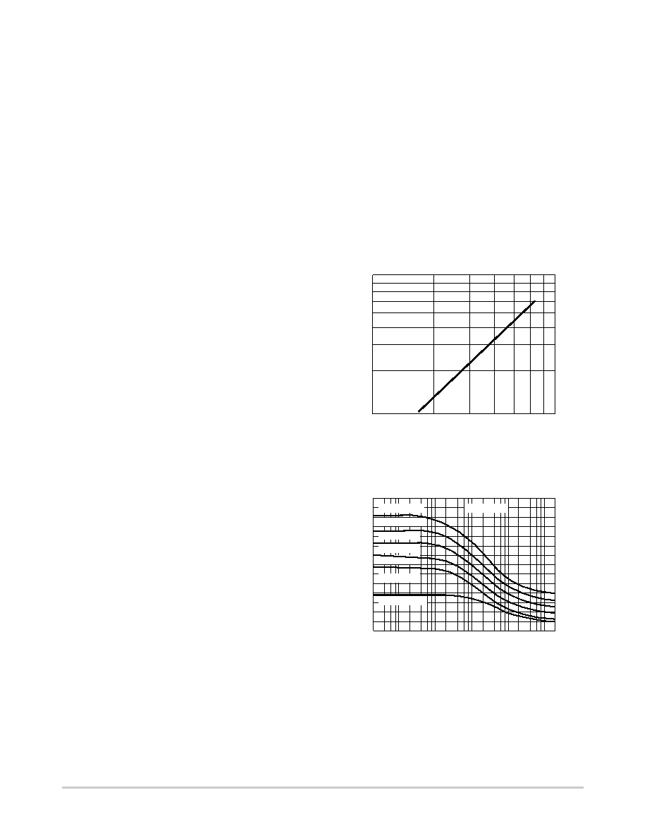
bandwidth versus ICC. As can be seen, the supply current can
be varied anywhere over the range of 100
mA to 600 mA for
a supply voltage of 1.8 V. An external resistor can be
inserted between the current control pin and the most
negative supply. The resistor can be selected between 1.0
W
to 100 k
W to provide any required supply current over the
indicated range. In addition, a small varying voltage on the
bias current control pin could be used for such exotic things
as changing the gainbandwidth for voltage controlled low
pass filters or amplitude modulation. Furthermore, control
over the slew rate and the rise time of the amplifier can be
obtained in the same manner. This control over the slew rate
also changes the settling time and overshoot in pulse
response applications. The settling time to 0.1% changes
from 5.0
ms at low bias to 2.0 ms at high bias. The supply
current control can also be utilized for waveshaping
applications such as for pulse or triangular waveforms. The
gainbandwidth can be varied from between 250 kHz at low
bias to 600 kHz at high bias current. The slew rate range is
0.08 V/
ms at low bias and 0.25 V/ms at high bias.
Figure 3. Unity Gain Bandwidth vs. Power Supply
Current for VCC = ±0.9 V
Figure 4. ICC Current vs. Bias Current Adjusting
Resistor for Several Supply Voltages
800
700
600
500
400
300
200
100
200
300
400 500 600700
UNITY GAIN BANDWIDTH (kHz)
TA 25°C
VCC 15V
VCC 12V
VCC 9V
VCC 6V
VCC 3V
VCC 2V
VCC 1.8V
1.4
1.2
1.0
0.8
0.6
0.4
0.2
0.0
100
101
102
103
104
105
RADJ (W)
POWER
SUPPL
Y
CURRENT
(m
A)
I CC
CURRENT
(mA)
相关PDF资料 |
PDF描述 |
|---|---|
| TMM-112-03-G-D | CONN HEADER 24POS DBL 2MM T/H |
| FTSH-108-04-L-DV-P | CONN HEADER 16POS DUAL .05" SMD |
| FTSH-108-01-L-DV-P | CONN HEADER 16POS DUAL .05" SMD |
| FTSH-120-01-F-DV-P-TR | CONN HEADER 40POS DUAL .05" SMD |
| FTSH-110-01-L-DV-EJ-TR | CONN UNSHROUDED HDR 20POS .05" |
相关代理商/技术参数 |
参数描述 |
|---|---|
| SA5230DR2 | 功能描述:运算放大器 - 运放 1.8V Single Rail to RoHS:否 制造商:STMicroelectronics 通道数量:4 共模抑制比(最小值):63 dB 输入补偿电压:1 mV 输入偏流(最大值):10 pA 工作电源电压:2.7 V to 5.5 V 安装风格:SMD/SMT 封装 / 箱体:QFN-16 转换速度:0.89 V/us 关闭:No 输出电流:55 mA 最大工作温度:+ 125 C 封装:Reel |
| SA5230DR2G | 功能描述:运算放大器 - 运放 1.8V Single Rail to Rail Industrial Temp RoHS:否 制造商:STMicroelectronics 通道数量:4 共模抑制比(最小值):63 dB 输入补偿电压:1 mV 输入偏流(最大值):10 pA 工作电源电压:2.7 V to 5.5 V 安装风格:SMD/SMT 封装 / 箱体:QFN-16 转换速度:0.89 V/us 关闭:No 输出电流:55 mA 最大工作温度:+ 125 C 封装:Reel |
| SA5230FE | 制造商:PHILIPS 制造商全称:NXP Semiconductors 功能描述:Low voltage operational amplifier |
| SA5230N | 功能描述:运算放大器 - 运放 1.8V Single Rail to RoHS:否 制造商:STMicroelectronics 通道数量:4 共模抑制比(最小值):63 dB 输入补偿电压:1 mV 输入偏流(最大值):10 pA 工作电源电压:2.7 V to 5.5 V 安装风格:SMD/SMT 封装 / 箱体:QFN-16 转换速度:0.89 V/us 关闭:No 输出电流:55 mA 最大工作温度:+ 125 C 封装:Reel |
| SA5230NG | 功能描述:运算放大器 - 运放 1.8V Single Rail to Rail Industrial Temp RoHS:否 制造商:STMicroelectronics 通道数量:4 共模抑制比(最小值):63 dB 输入补偿电压:1 mV 输入偏流(最大值):10 pA 工作电源电压:2.7 V to 5.5 V 安装风格:SMD/SMT 封装 / 箱体:QFN-16 转换速度:0.89 V/us 关闭:No 输出电流:55 mA 最大工作温度:+ 125 C 封装:Reel |
发布紧急采购,3分钟左右您将得到回复。