参数资料
| 型号: | SA5230DG |
| 厂商: | ON Semiconductor |
| 文件页数: | 4/18页 |
| 文件大小: | 0K |
| 描述: | IC OPAMP LOW VOLTAGE 8-SOIC |
| 标准包装: | 98 |
| 放大器类型: | 通用 |
| 电路数: | 1 |
| 输出类型: | 满摆幅 |
| 转换速率: | 0.25 V/µs |
| 增益带宽积: | 600kHz |
| 电流 - 输入偏压: | 40nA |
| 电压 - 输入偏移: | 400µV |
| 电流 - 电源: | 1.1mA |
| 电流 - 输出 / 通道: | 32mA |
| 电压 - 电源,单路/双路(±): | 1.8 V ~ 15 V,±0.9 V ~ 7.5 V |
| 工作温度: | -40°C ~ 85°C |
| 安装类型: | 表面贴装 |
| 封装/外壳: | 8-SOIC(0.154",3.90mm 宽) |
| 供应商设备封装: | 8-SOICN |
| 包装: | 管件 |
NE5230, SA5230, SE5230
http://onsemi.com
12
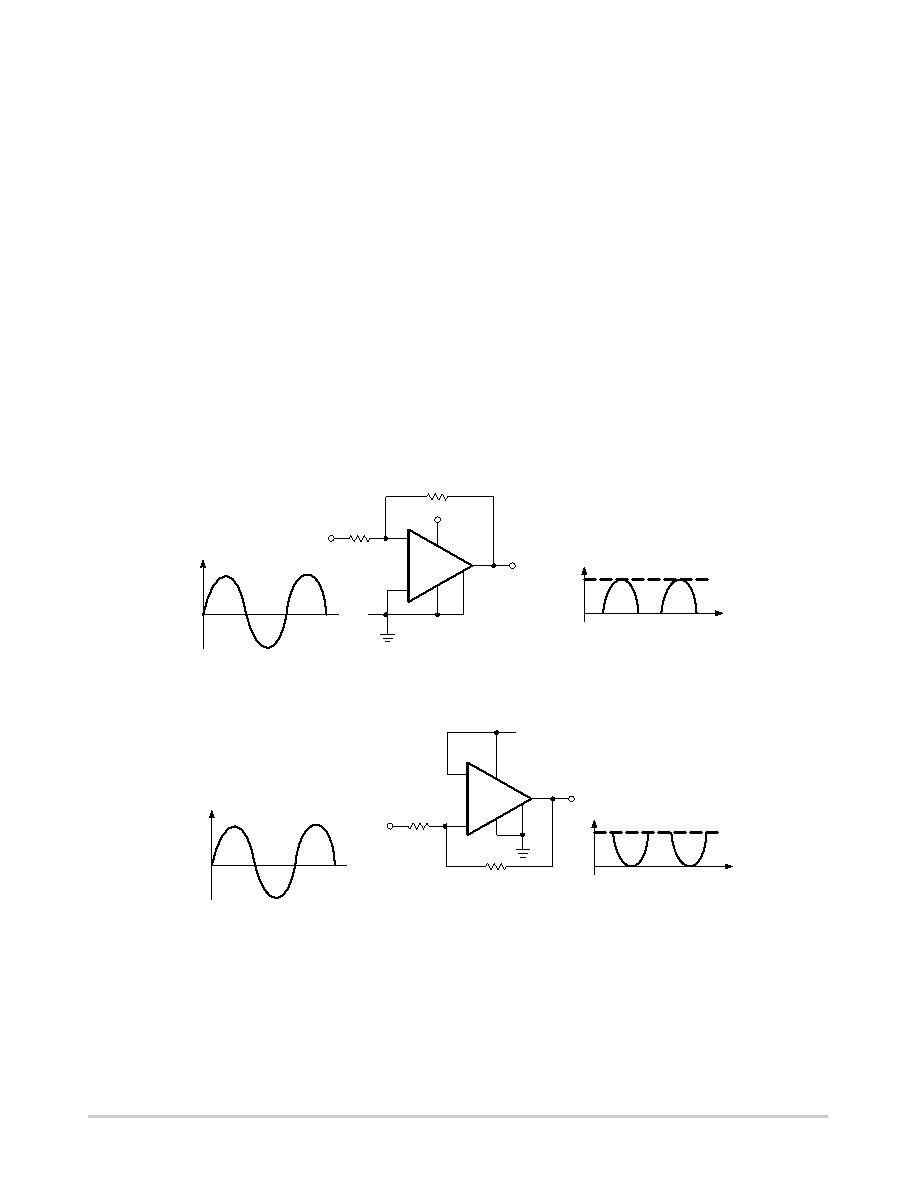
HALFWAVE RECTIFIER WITH
RAILTOGROUND OUTPUT SWING
Since the NE5230 input commonmode range includes
both positive and negative supply rails and the output can
also swing to either supply, achieving halfwave rectifier
functions in either direction becomes a simple task. All that
is needed are two external resistors; there is no need for
diodes or matched resistors. Moreover, it can have either
positive or negativegoing outputs, depending on the way
the bias is arranged. In Figure 9, the circuit is biased to
ground, while circuit (Figure 10) is biased to the positive
supply. This rather unusual biasing does not cause any
problems with the NE5230 because of the unique internal
saturation detectors incorporated into the part to keep the
PNP and NPN output transistors out of “hard” saturation. It
is therefore relatively quick to recover from a saturated
output condition. Furthermore, the device does not have
parasitic current draw when the output is biased to either rail.
This makes it possible to bias the NE5230 into “saturation”
and obtain halfwave rectification with good recovery. The
simplicity of biasing and the railtoground halfsine wave
swing are unique to this device. The circuit gain can be
changed by the standard op amp gain equations for an
inverting configuration.
It can be seen in these configurations that the op amp
cannot respond to onehalf of the incoming waveform. It
cannot respond because the waveform forces the amplifier
to swing the output beyond either ground or the positive
supply rail, depending on the biasing, and, also, the output
cannot disengage during this half cycle. During the other
half cycle, however, the amplifier achieves a halfwave that
can have a peak equal to the total supply voltage. The
photographs in Figure 11 show the effect of the different
biasing schemes, as well as the wide bandwidth (it works
over the full audio range), that the NE5230 can achieve in
this configuration.
VCC
Figure 9. RailtoGround Output Swing Referenced to Ground
Figure 10. NegativeGoing Output Referenced to VCC
VIN
VCC
2
3
4
5
6
7
+
O
t
VCC
VOUT
t
VCC
3
2
4
5
6
7
VIN
VOUT
VCC
+
HalfWave Rectifier With PositiveGoing Output Swings
10W
相关PDF资料 |
PDF描述 |
|---|---|
| TMM-112-03-G-D | CONN HEADER 24POS DBL 2MM T/H |
| FTSH-108-04-L-DV-P | CONN HEADER 16POS DUAL .05" SMD |
| FTSH-108-01-L-DV-P | CONN HEADER 16POS DUAL .05" SMD |
| FTSH-120-01-F-DV-P-TR | CONN HEADER 40POS DUAL .05" SMD |
| FTSH-110-01-L-DV-EJ-TR | CONN UNSHROUDED HDR 20POS .05" |
相关代理商/技术参数 |
参数描述 |
|---|---|
| SA5230DR2 | 功能描述:运算放大器 - 运放 1.8V Single Rail to RoHS:否 制造商:STMicroelectronics 通道数量:4 共模抑制比(最小值):63 dB 输入补偿电压:1 mV 输入偏流(最大值):10 pA 工作电源电压:2.7 V to 5.5 V 安装风格:SMD/SMT 封装 / 箱体:QFN-16 转换速度:0.89 V/us 关闭:No 输出电流:55 mA 最大工作温度:+ 125 C 封装:Reel |
| SA5230DR2G | 功能描述:运算放大器 - 运放 1.8V Single Rail to Rail Industrial Temp RoHS:否 制造商:STMicroelectronics 通道数量:4 共模抑制比(最小值):63 dB 输入补偿电压:1 mV 输入偏流(最大值):10 pA 工作电源电压:2.7 V to 5.5 V 安装风格:SMD/SMT 封装 / 箱体:QFN-16 转换速度:0.89 V/us 关闭:No 输出电流:55 mA 最大工作温度:+ 125 C 封装:Reel |
| SA5230FE | 制造商:PHILIPS 制造商全称:NXP Semiconductors 功能描述:Low voltage operational amplifier |
| SA5230N | 功能描述:运算放大器 - 运放 1.8V Single Rail to RoHS:否 制造商:STMicroelectronics 通道数量:4 共模抑制比(最小值):63 dB 输入补偿电压:1 mV 输入偏流(最大值):10 pA 工作电源电压:2.7 V to 5.5 V 安装风格:SMD/SMT 封装 / 箱体:QFN-16 转换速度:0.89 V/us 关闭:No 输出电流:55 mA 最大工作温度:+ 125 C 封装:Reel |
| SA5230NG | 功能描述:运算放大器 - 运放 1.8V Single Rail to Rail Industrial Temp RoHS:否 制造商:STMicroelectronics 通道数量:4 共模抑制比(最小值):63 dB 输入补偿电压:1 mV 输入偏流(最大值):10 pA 工作电源电压:2.7 V to 5.5 V 安装风格:SMD/SMT 封装 / 箱体:QFN-16 转换速度:0.89 V/us 关闭:No 输出电流:55 mA 最大工作温度:+ 125 C 封装:Reel |
发布紧急采购,3分钟左右您将得到回复。