- 您现在的位置:买卖IC网 > PDF目录225144 > SA56615-46D (NXP SEMICONDUCTORS) 1-CHANNEL POWER SUPPLY SUPPORT CKT, PDSO5 PDF资料下载
参数资料
| 型号: | SA56615-46D |
| 厂商: | NXP SEMICONDUCTORS |
| 元件分类: | 电源管理 |
| 英文描述: | 1-CHANNEL POWER SUPPLY SUPPORT CKT, PDSO5 |
| 封装: | 1.50 MM, PLASTIC, SOT-23, SOT-25, SO-5 |
| 文件页数: | 13/23页 |
| 文件大小: | 244K |
| 代理商: | SA56615-46D |
Philips Semiconductors
Product data
SA56615-XX;
SA56616-XX
CMOS system reset with adjustable delay time
2003 Oct 15
20
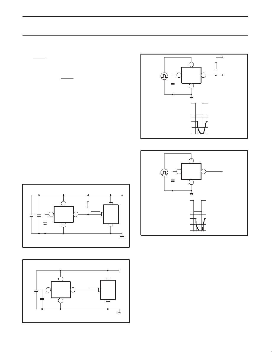
APPLICATION INFORMATION
The SA56615-XX differs from the SA56616-XX in that it requires a
VOUT (RESET) pull-up resistor from pin 1 to VDD. Typical value for
RPU, the pull-up resistor, is 470 k.
The reset delay time is the duration measured from the time VDD
exceeds the upper detection threshold (VSH) and when reset
release occurs (VOUT or RESET goes HIGH).
Figures 76 and 77 show typical application circuits for the
SA56615-XX and SA56616-XX in which the delay time is externally
adjusted by a capacitor connected from CD (pin 5) to ground. The
delay time may be varied from 150 ns to 1 second with the
appropriate external capacitor. Typical capacitor value is from
100 pF to 1
F. Refer to “Delay time versus CD” in Typical
Performance Curves for the various detection threshold voltages.
The delay time is approximated by
tD 1.2 × RD × CD
where:
RD is CD pin resistance (typically 1 M)
CD is the external delay time capacitor
The CD (delay pin) threshold voltage, VTCD is typically 0.5 × VDD.
Figures 78 and 79 show the test circuits that are used to measure
the reset delay time of the SA56615-XX and SA56616-XX
respectively. The delay diagrams indicate how the measurement is
to be made. The input voltage, VIN is switched from VSH + 2.0 V to
0.7 V. The delay time is measured from the falling edge of VIN to
where the CD (delay pin) threshold voltage is 0.5 × VDD.
VIN
2
1
3
5
SA56615-XX
OUT
GND
CD
VDD
LOGIC
SYSTEM
RESET
VDD
SL01596
RPU
Figure 76. SA56615-XX application circuit.
SL01597
VIN
2
1
3
5
SA56616-XX
OUT
GND
CD
VDD
LOGIC
SYSTEM
RESET
VDD
Figure 77. SA56616-XX application circuit.
VIN
2
1
3
5
SA56615-XX
OUT
GND
CD
VDD
+5 V
470 k
CD
SL01601
VSH +2.0 V
0.7 V
GND
50%
INPUT VOLTAGE
OUTPUT VOLTAGE
100%
Figure 78. SA56615-XX delay time, tD test circuit and diagram.
VIN
2
1
3
5
SA56616-XX
OUT
GND
CD
VDD
CD
SL01602
VSH +2.0 V
0.7 V
GND
50%
INPUT VOLTAGE
OUTPUT VOLTAGE
100%
Figure 79. SA56616-XX delay time, tD test circuit and diagram.
相关PDF资料 |
PDF描述 |
|---|---|
| SA56615-27D | 1-CHANNEL POWER SUPPLY SUPPORT CKT, PDSO5 |
| SA57250-33GW-G | 0.3 A SWITCHING REGULATOR, 57.5 kHz SWITCHING FREQ-MAX, PDSO5 |
| SA58631TK | 3 W BTL audio amplifier |
| SA58632BS | 2 x 2.2 W BTL audio amplifier |
| SA58635UK | 2 x 25 mW class-G stereo headphone driver with I2C-bus volume control |
相关代理商/技术参数 |
参数描述 |
|---|---|
| SA5664 | 制造商:SILAN 制造商全称:Silan Microelectronics Joint-stock 功能描述:3-PHASE SPINDLE MOTOR DRIVER FOR CD-ROM |
| SA568A | 制造商:PHILIPS 制造商全称:NXP Semiconductors 功能描述:150MHz phase-locked loop |
| SA568AD | 制造商:PHILIPS 制造商全称:NXP Semiconductors 功能描述:150MHz phase-locked loop |
| SA568AN | 制造商:PHILIPS 制造商全称:NXP Semiconductors 功能描述:150MHz phase-locked loop |
| SA56EX | 功能描述:功率放大器 IC 60V 5A PULSE WDTH MODULATION AMP RoHS:否 制造商:TriQuint Semiconductor 封装 / 箱体: 工作电源电压:28 V 电源电流:2.5 A 工作温度范围: 封装: |
发布紧急采购,3分钟左右您将得到回复。