- 您现在的位置:买卖IC网 > PDF目录192316 > SCAN182245ASSC (FAIRCHILD SEMICONDUCTOR CORP) PDF资料下载
参数资料
| 型号: | SCAN182245ASSC |
| 厂商: | FAIRCHILD SEMICONDUCTOR CORP |
| 元件分类: | 总线收发器 |
| 中文描述: | SCAN/JTAG/3J SERIES, DUAL 9-BIT BOUNDARY SCAN TRANSCEIVER, TRUE OUTPUT, PDSO56 |
| 封装: | 0.300 INCH, MO-118, SSOP-56 |
| 文件页数: | 12/13页 |
| 文件大小: | 133K |
| 代理商: | SCAN182245ASSC |
www.fairchildsemi.com
8
SCAN18224
5A
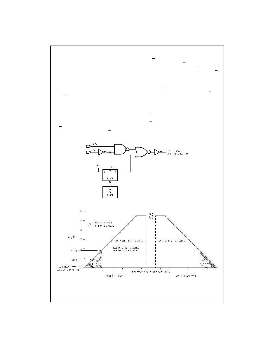
SCAN ABT Live Insertion and Power Cycling Characteristics
SCAN ABT is intended to serve in Live Insertion backplane
applications. It provides 2nd Level Isolation1 which indi-
cates that while external circuitry to control the output
enable pin is unnecessary, there may be a need to imple-
ment differential length backplane connector pins for VCC
and GND. As well, pre-bias circuitry for backplane pins
may be necessary to avoid capacitive loading effects dur-
ing live insertion.
SCAN ABT provides control of output enable pins during
power cycling via the circuit in Figure 1. It essentially con-
trols the Gn pin until VCC reaches a known level.
During power-up, when VCC ramps through the 0.0V to
0.7V range, all internal device circuitry is inactive, leaving
output and I/O pins of the device in high impedance. From
approximately 0.8V to 1.8V VCC, the Power-On-Reset cir-
cuitry, (POR), in Figure 1 becomes active and maintains
device high impedance mode. The POR does this by pro-
viding a low from its output that resets the flip-flop The out-
put, Q, of the flip-flop then goes high and disables the NOR
gate from an incidental low input on the Gn pin. After 1.8V
VCC, the POR circuitry becomes inactive and ceases to
control the flip-flop. To bring the device out of high imped-
ance, the Gn input must receive an inactive-to-active transi-
tion, a high-to-low transition on Gn in this case to change
the state of the flip-flop. With a low on the Q output of the
flip-flop, the NOR gate is free to allow propagation of a Gn
signal.
During power-down, the Power-On-Reset circuitry will
become active and reset the flip-flop at approximately 1.8V
VCC. Again, the Q output of the flip-flop returns to a high
and disables the NOR gate from inputs from the Gn pin.
The device will then remain in high impedance for the
remaining ramp down from 1.8V to 0.0V VCC.
Some suggestions to help the designer with live insertion
issues:
The Gn pin can float during power-up until the Power-
On-Reset circuitry becomes inactive.
The Gn pin can float on power-down only after the
Power-On-Reset has become active.
The description of the functionality of the Power-On-Reset
circuitry can best be described in the diagram of Figure 2.
FIGURE 1.
1Section 7, “Design Consideration for Fault Tolerant Backplanes”, Application Note AN-881.
SCAN ABT includes additional power-on reset circuitry not otherwise included in ABT devices.
FIGURE 2.
相关PDF资料 |
PDF描述 |
|---|---|
| SCAN182245AMTDX | |
| SCAN182374ASSC | |
| SCAN182374ASSCX | |
| SCAN18374TSSCX | |
| SCANPSC100FSCX | |
相关代理商/技术参数 |
参数描述 |
|---|---|
| SCAN182245ASSCQB | 制造商:NSC 制造商全称:National Semiconductor 功能描述:Non-Inverting Transceiver with 25OHM Series Resistor Outputs |
| SCAN182245ASSCX | 功能描述:总线收发器 Non-Inverting Trans RoHS:否 制造商:Fairchild Semiconductor 逻辑类型:CMOS 逻辑系列:74VCX 每芯片的通道数量:16 输入电平:CMOS 输出电平:CMOS 输出类型:3-State 高电平输出电流:- 24 mA 低电平输出电流:24 mA 传播延迟时间:6.2 ns 电源电压-最大:2.7 V, 3.6 V 电源电压-最小:1.65 V, 2.3 V 最大工作温度:+ 85 C 封装 / 箱体:TSSOP-48 封装:Reel |
| SCAN182245ASSMQB | 制造商:NSC 制造商全称:National Semiconductor 功能描述:Non-Inverting Transceiver with 25OHM Series Resistor Outputs |
| SCAN182245ASSMX | 制造商:NSC 制造商全称:National Semiconductor 功能描述:Non-Inverting Transceiver with 25OHM Series Resistor Outputs |
| SCAN182245BFCQB | 制造商:NSC 制造商全称:National Semiconductor 功能描述:Non-Inverting Transceiver with 25OHM Series Resistor Outputs |
发布紧急采购,3分钟左右您将得到回复。