- 您现在的位置:买卖IC网 > PDF目录11822 > SCC2692AC1N28,129 (NXP Semiconductors)IC DUART 28-DIP PDF资料下载
参数资料
| 型号: | SCC2692AC1N28,129 |
| 厂商: | NXP Semiconductors |
| 文件页数: | 17/30页 |
| 文件大小: | 0K |
| 描述: | IC DUART 28-DIP |
| 标准包装: | 13 |
| 特点: | 故障启动位检测 |
| 通道数: | 2,DUART |
| FIFO's: | 3 位 |
| 电源电压: | 5V |
| 带并行端口: | 是 |
| 带自动流量控制功能: | 是 |
| 带故障启动位检测功能: | 是 |
| 带CMOS: | 是 |
| 安装类型: | 通孔 |
| 封装/外壳: | 28-DIP(0.600",15.24mm) |
| 供应商设备封装: | 28-DIP |
| 包装: | 管件 |
| 其它名称: | 933981720129 SCC2692AC1N28-S SCC2692AC1N28-S-ND |
第1页第2页第3页第4页第5页第6页第7页第8页第9页第10页第11页第12页第13页第14页第15页第16页当前第17页第18页第19页第20页第21页第22页第23页第24页第25页第26页第27页第28页第29页第30页
Philips Semiconductors
Product specification
SCC2692
Dual asynchronous receiver/transmitter (DUART)
1998 Sep 04
24
INTRN
D0–D7
TxDA/B
OP0–OP7
150pF
2.15V
750
50pF
+5V
2.7K
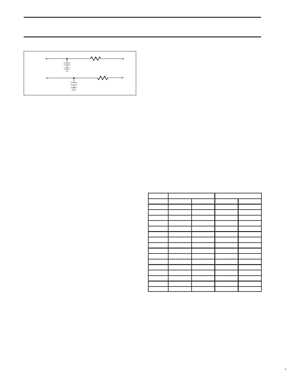
SD00143
Figure 13. Test Conditions on Outputs
Output Port Notes
The output ports are controlled from four places: the OPCR register,
the OPR register, the MR registers and the command register. The
OPCR register controls the source of the data for the output ports
OP2 through OP7. The data source for output ports OP0 and OP1 is
controlled by the MR and CR registers. When the OPR is the source
of the data for the output ports, the data at the ports is inverted from
that in the OPR register. The content of the OPR register is
controlled by the “Set Output Port Bits Command” and the “Reset
Output Bits Command”. These commands are at E and F,
respectively. When these commands are used, action takes place
only at the bit locations where ones exist. For example, a one in bit
location 5 of the data word used with the “Set Output Port Bits”
command will result in OPR5 being set to one. The OP5 would then
be set to zero (VSS). Similarly, a one in bit position 5 of the data
word associated with the “Reset Output Ports Bits” command would
set OPR5 to zero and, hence, the pin OP5 to a one (VDD).
The CTS, RTS, CTS Enable Tx signals
CTS (Clear To Send) is usually meant to be a signal to the
transmitter meaning that it may transmit data to the receiver. The
CTS input is on pin IP0 for TxA and on IP1 for TxB. The CTS signal
is active low; thus, it is called CTSAN for TxA and CTSBN for TxB.
RTS is usually meant to be a signal from the receiver indicating that
the receiver is ready to receive data. It is also active low and is,
thus, called RTSAN for RxA and RTSBN for RxB. RTSAN is on pin
OP0 and RTSBN is on OP1. A receiver’s RTS output will usually be
connected to the CTS input of the associated transmitter. Therefore,
one could say that RTS and CTS are different ends of the same
wire!
MR2(4) is the bit that allows the transmitter to be controlled by the
CTS pin (IP0 or IP1). When this bit is set to one AND the CTS input
is driven high, the transmitter will stop sending data at the end of the
present character being serialized. It is usually the RTS output of the
receiver that will be connected to the transmitter’s CTS input. The
receiver will set RTS high when the receiver FIFO is full AND the
start bit of the fourth character is sensed. Transmission then stops
with four valid characters in the receiver. When MR2(4) is set to one,
CTSN must be at zero for the transmitter to operate. If MR2(4) is set
to zero, the IP pin will have no effect on the operation of the
transmitter.
MR1(7) is the bit that allows the receiver to control OP0. When OP0
(or OP1) is controlled by the receiver, the meaning of that pin will be
RTS. However, a point of confusion arises in that OP0 (or OP1) may
also be controlled by the transmitter. When the transmitter is
controlling this pin, its meaning is not RTS at all. It is, rather, that the
transmitter has finished sending its last data byte. Programming the
OP0 or OP1 pin to be controlled by the receiver and the transmitter
at the same time is allowed, but would usually be incompatible.
RTS can also be controlled by the commands 1000 and 1001 in the
command register. RTS is expressed at the OP0 or OP1 pin which
is still an output port. Therefore, the state of OP0 or OP1 should be
set low (either by commands of the CR register or by writing to the
Set Output Ports Register) for the receiver to generate the proper
RTS signal. The logic at the output is basically a NAND of the OPR
register and the RTS signal as generated by the receiver. When the
RTS flow control is selected via the MR(7) bit state of the OPR
register is not changed. Terminating the use of “Flow Control” (via
the MR registers) will return the OP0 or OP1 pins to the control of
the OPR register.
Transmitter Disable Note
The sequence of instructions enable transmitter — load transmit
holding register — disable transmitter will result in nothing being
sent if the time between the end of loading the transmit holding
register and the disable command is less that 3/16 bit time in the
16x mode or one bit time in the 1x mode. Also, if the transmitter,
while in the enabled state and underrun condition, is immediately
disabled after a single character is loaded to the transmit holding
register, that character will not be sent.
In general, when it is desired to disable the transmitter before the
last character is sent AND the TxEMT bit is set in the status register
(TxEMT is always set if the transmitter has underrun or has just
been enabled), be sure the TxRDY bit is active immediately before
issuing the transmitter disable instruction. TxRDY sets at the end of
the “start bit” time. It is during the start bit that the data in the
transmit holding register is transferred to the transmit shift register.
Table 6.
Baud Rates Extended
Normal BRG
BRG Test
CSR[7:4]
ACR[7] = 0
ACR[7] = 1
ACR[7] = 0
ACR[7] = 1
0000
50
75
4,800
7,200
0001
110
880
0010
134.5
1,076
0011
200
150
19.2K
14.4K
0100
300
28.8K
0101
600
57.6K
0110
1,200
115.2K
0111
1,050
2,000
1,050
2,000
1000
2,400
57.6K
1001
4,800
1010
7,200
1,800
57.6K
14.4K
1011
9,600
1100
38.4K
19.2K
38.4K
19.2K
1101
Timer
1110
I/O2 – 16X
1111
I/O2 – 1X
NOTE:
Each read on address H‘2’ will toggle the baud rate test mode.
When in the BRG test mode, the baud rates change as shown to the
left. This change affects all receivers and transmitters on the DUART.
See
“Extended baud rates for SCN2681, SCN68681, SCC2691,
SCC2692, SCC68681 and SCC2698B” in application notes
elsewhere in this publication
The test mode at address H‘A’ changes all transmitters and
receivers to the 1x mode and connects the output ports to some
internal nodes.
相关PDF资料 |
PDF描述 |
|---|---|
| SCC2692AC1A44,529 | IC DUART SOT187-2 |
| VI-B5D-IY | CONVERTER MOD DC/DC 85V 50W |
| SC26C92C1A,529 | IC DUART SOT187-2 |
| SC16C554BIBM,128 | IC UART QUAD SOT414-1 |
| SCC68692E1A44,518 | IC DUART 44PLCC |
相关代理商/技术参数 |
参数描述 |
|---|---|
| SCC2692AC1N28-S | 功能描述:UART 接口集成电路 5V INDSTRL UART 2 C RoHS:否 制造商:Texas Instruments 通道数量:2 数据速率:3 Mbps 电源电压-最大:3.6 V 电源电压-最小:2.7 V 电源电流:20 mA 最大工作温度:+ 85 C 最小工作温度:- 40 C 封装 / 箱体:LQFP-48 封装:Reel |
| SCC2692AC1N40 | 制造商:NXP Semiconductors 功能描述:IC DUART 2692 DIP40 制造商:NXP Semiconductors 功能描述:IC, DUART, 2692, DIP40 制造商:NXP Semiconductors 功能描述:IC, DUAL UART, FIFO, 115KBAUD 5.5V DIP40; No. of Channels:2; Data Rate:1Mbps; Supply Voltage Min:4.5V; Supply Voltage Max:5.5V; Digital IC Case Style:DIP; No. of Pins:40; Operating Temperature Min:0C; Operating Temperature Max:70C ;RoHS Compliant: Yes |
| SCC2692AC1N40,602 | 功能描述:UART 接口集成电路 2CH. 5V IND. UART RoHS:否 制造商:Texas Instruments 通道数量:2 数据速率:3 Mbps 电源电压-最大:3.6 V 电源电压-最小:2.7 V 电源电流:20 mA 最大工作温度:+ 85 C 最小工作温度:- 40 C 封装 / 箱体:LQFP-48 封装:Reel |
| SCC2692AC1N40602 | 制造商:NXP Semiconductors 功能描述:IC DUAL UART FIFO 1MBPS 5.5V DIP-40 |
| SCC2692AE1A44 | 功能描述:UART 接口集成电路 5V INDSTRL UART 2 C RoHS:否 制造商:Texas Instruments 通道数量:2 数据速率:3 Mbps 电源电压-最大:3.6 V 电源电压-最小:2.7 V 电源电流:20 mA 最大工作温度:+ 85 C 最小工作温度:- 40 C 封装 / 箱体:LQFP-48 封装:Reel |
发布紧急采购,3分钟左右您将得到回复。