- 您现在的位置:买卖IC网 > PDF目录98079 > SED1336F0A 640 X 256 DOTS DOT MAT LCD DSPL CTLR, PQFP60 PDF资料下载
参数资料
| 型号: | SED1336F0A |
| 元件分类: | 显示控制器 |
| 英文描述: | 640 X 256 DOTS DOT MAT LCD DSPL CTLR, PQFP60 |
| 封装: | PLASTIC, QFP6-60 |
| 文件页数: | 7/12页 |
| 文件大小: | 50K |
| 代理商: | SED1336F0A |
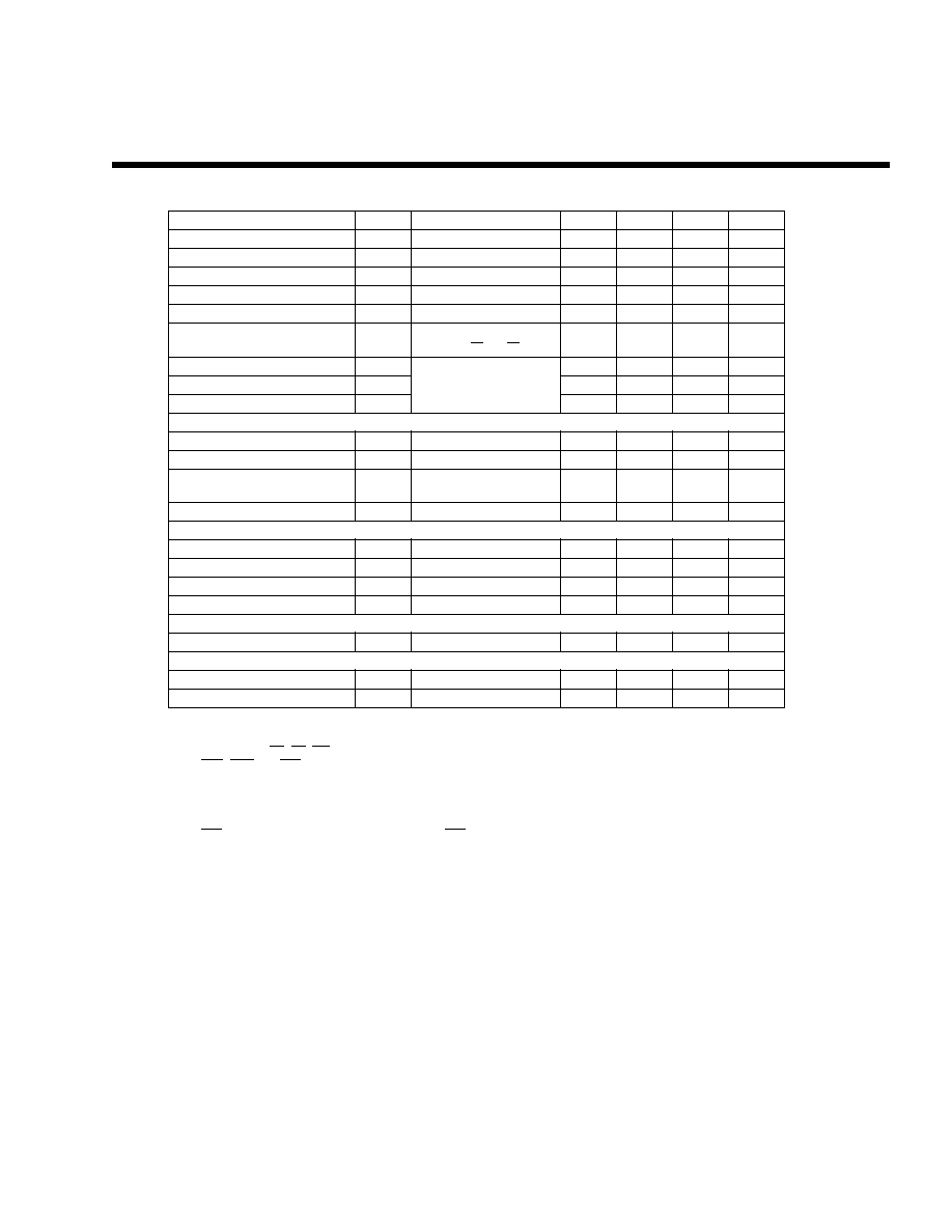
156
DC Electrical Characteristics
Parameter
Symbol
Condition
Min
Typ
Max
Unit
Supply voltage
VDD
4.5
5.0
5.5
V
Register data retention voltage
VHO
2.0
—
6.0
V
Input leakage current
ILI
VI = VDD. See note 6.
—
0.05
2.0
A
Output leakage current
ILO
VI = VSS. See note 6.
—
0.10
5.0
A
Operating supply current
Iopr
See note 4.
—
11
15
mA
Quiescent supply current
IQ
Sleep mode,
—
0.05
20.0
A
VOSC1 = VCS = VRD = VDD
Oscillator frequency
fOSC
1.0
—
10.0
MHz
External clock frequency
fCL
1.0
—
10.0
MHz
Oscillator feedback resistance
Rf
0.5
1.0
3.0
M
TTL
HIGH-level input voltage
VIHT
See note 1.
0.8VDD
—VDD
V
LOW-level input voltage
VILT
See note 1.
VSS
—
0.2VDD
V
HIGH-level output voltage
VOHT
IOH = –5.0 mA.
2.4
—
V
See note 1.
LOW-level output voltage
VOLT
IOL = 5.0 mA. See note 1.
—
VSS + 0.4
V
CMOS
HIGH-level input voltage
VIHC
See note 2.
0.8VDD
—VDD
V
LOW-level input voltage
VILC
See note 2.
VSS
—
0.2VDD
V
HIGH-level output voltage
VOHC
IOH = –2.0 mA. See note 2. VDD – 0.4
—
V
LOW-level output voltage
VOLC
IOH = 1.6 mA. See note 2.
—
VSS + 0.4
V
Open-drain
LOW-level output voltage
VOLN
IOL = 6.0 mA. See note 5.
—
VSS + 0.4
V
Schmitt-trigger
Rising-edge threshold voltage
VT+
See note 3.
0.5VDD
0.7VDD
0.8VDD
V
Falling-edge threshold voltage
VT–
See note 3.
0.2VDD
0.3VDD
0.5VDD
V
Notes:
1. D0 to D7, A0, CS, RD, WR, VD0 to VD7, VA0 to VA15,
VRD, VWR and VCE are TTL-level inputs.
2. SEL1 and NT/PL are CMOS-level inputs. YD, XD0 to
XD3, XSCL, LP, WF, YDIS and CLO are CMOS-level
outputs.
3. RES is a Schmitt-trigger input. The pulsewidth on RES
must be at least 200
s. Note that pulses of more than a
few seconds will cause DC voltages to be applied to the
LCD panel.
4. fOSC = 10 MHz, no load (no display memory), internal
character generator, 256
× 200 pixel display. The operat-
ing supply current can be reduced by approximately 1 mA
by setting both CLO and the display OFF.
5. SNC and VSD are n-channel, open-drain outputs. The
voltage on the outputs should not exceed VDD as internal
diodes connect the pins to VDD (SED1336F only).
6. VD0 to VD7 and D0 to D7 have internal feedback circuits
so that if the inputs become high-impedance, the input
state immediately prior to that is held. Because of the
feedback circuit, input current flow occurs when the
inputs are in an intermediate state.
7. Because the oscillator circuit input bias current is in the
order of
A, design the printed circuit board so as to
reduce leakage currents.
VDD = 4.5 to 5.5V, VSS = 0V, Ta = –20 to 75
°C
Measured at crystal,
47.5% duty cycle.
See note 7.
SED1336
相关PDF资料 |
PDF描述 |
|---|---|
| SED1345F0A | 640 X 480 DOTS CRT TO LCD CONV DSPL CTLR, PQFP80 |
| SED1351F0A | 1024 X 512 DOTS DOT MAT LCD DSPL CTLR, PQFP100 |
| SED1351F0A | DOT MAT LCD DSPL CTLR, PQFP100 |
| SED1352 | 640 X 480 PIXELS DOT MAT LCD DSPL CTLR, PQFP100 |
| SH1475IMLTRT | SPECIALTY MICROPROCESSOR CIRCUIT, PQCC36 |
相关代理商/技术参数 |
参数描述 |
|---|---|
| SED1351 | 制造商:未知厂家 制造商全称:未知厂家 功能描述:GRAPHICS LCD CONTROLLER |
| SED1351F | 制造商:未知厂家 制造商全称:未知厂家 功能描述:CMOS GRAPHIC LCD CONTROLLER |
| SED1351F0A | 制造商:Seiko Instruments Inc (SII) 功能描述: |
| SED1352 | 制造商:EPSON 制造商全称:EPSON 功能描述:Document Number: X16B-Q-001-06 |
| SED1353 | 制造商:EPSON 制造商全称:EPSON 功能描述:SED1353 GRAPHICS LCD CONTROLLER |
发布紧急采购,3分钟左右您将得到回复。