- 您现在的位置:买卖IC网 > PDF目录48773 > SFC3.3-4.BCT 150 W, UNIDIRECTIONAL, 4 ELEMENT, SILICON, TVS DIODE, MO-211BB PDF资料下载
参数资料
| 型号: | SFC3.3-4.BCT |
| 元件分类: | TVS二极管 - 瞬态电压抑制 |
| 英文描述: | 150 W, UNIDIRECTIONAL, 4 ELEMENT, SILICON, TVS DIODE, MO-211BB |
| 封装: | 1.50 X 1 MM, LEAD FREE, MO-211, FLIP CHIP-6 |
| 文件页数: | 4/7页 |
| 文件大小: | 230K |
| 代理商: | SFC3.3-4.BCT |
4
2008 Semtech Corp.
www.semtech.com
PRELIMINARY
PROTECTION PRODUCTS
SFC3.3-4
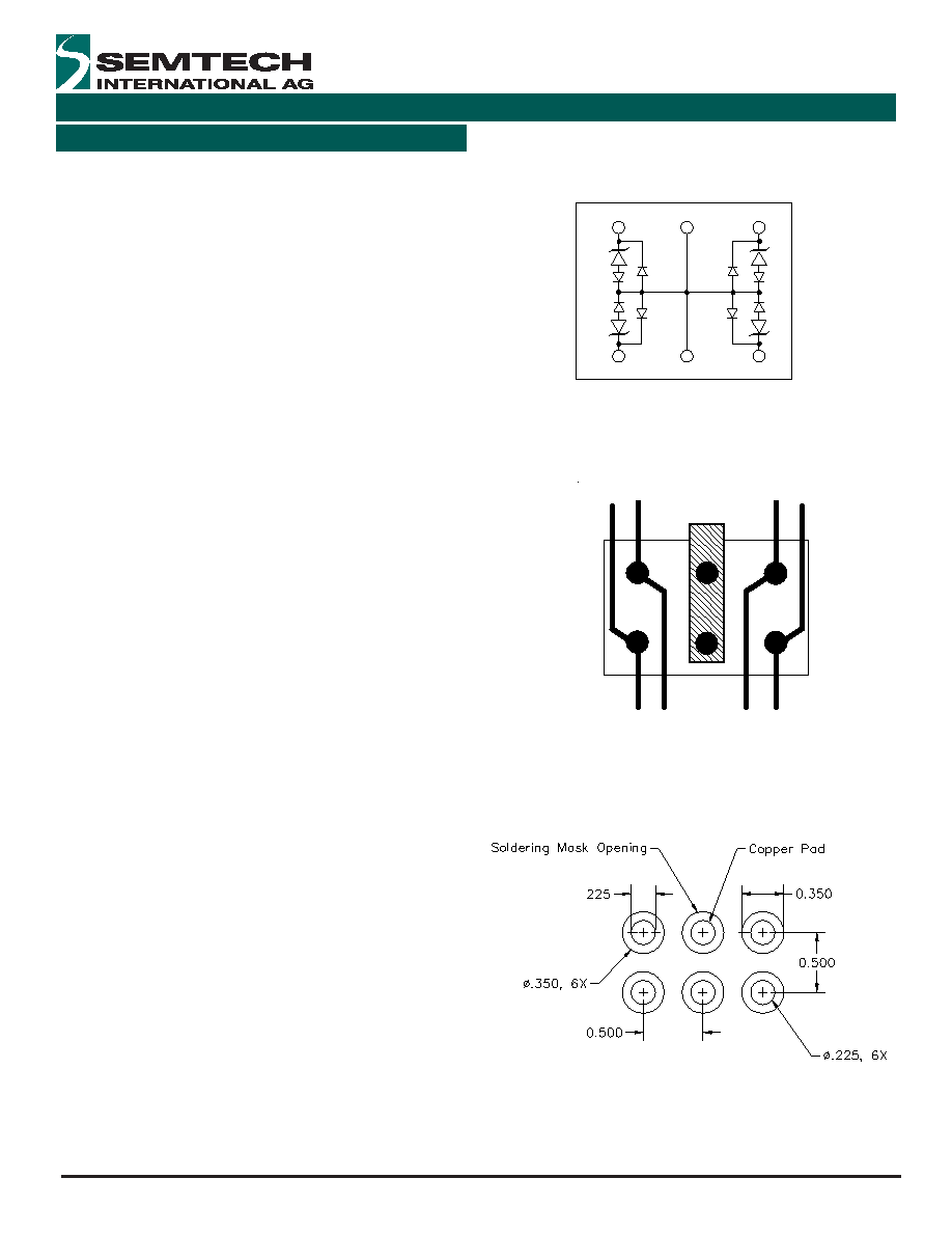
Device Schematic and Pin Configuration
Layout Example
NSMD Package Footprint
Device Connection Options
The SFC3.3-4 has solder bumps located in a 3 x 2
matrix layout on the active side of the device. The
bumps are designated by the numbers 1 - 3 along the
horizontal axis and letters A - B along the vertical axis.
The lines to be protected are connected at bumps A1,
B1, A3, and B3. Bumps A2 and B2 are connected to
ground. All path lengths should be kept as short as
possible to minimize the effects of parasitic inductance
in the board traces.
Due to the “snap-back” characteristics of the low
voltage TVS, it is not recommended that any of the I/O
bumps be directly connected to a DC source greater
than snap-back votlage (V
SB) as the device can latch on
as described the EPD TVS characteristics section.
Flip Chip TVS
Flip chip TVS devices are wafer level chip scale pack-
ages. They eliminate external plastic packages and
leads and thus result in a significant board space
savings. Manufacturing costs are minimized since they
do not require an intermediate level interconnect or
interposer layer for reliable operation. They are com-
patible with current pick and place equipment further
reducing manufacturing costs. Certain precautions
and design considerations have to be observed how-
ever for maximum solder joint reliability. These include
solder pad definition, board finish, and assembly
parameters.
Printed Circuit Board Mounting
Non-solder mask defined (NSMD) land patterns are
recommended for mounting the SFC3.3-4. Solder
mask defined (SMD) pads produce stress points near
the solder mask on the PCB side that can result in
solder joint cracking when exposed to extreme fatigue
conditions. The recommended pad size is 0.225 ±
0.010 mm with a solder mask opening of 0.350 ±
0.025 mm.
Printed Circuit Board Finish
A uniform board finish is critical for good assembly
yield. Two finishes that provide uniform surface coat-
ings are immersion nickel gold and organic surface
protectant (OSP). A non-uniform finish such as hot air
solder leveling (HASL) can lead to mounting problems
To Protected IC
To Connector
Ground
Applications Information
6
54
12
3
A
B
相关PDF资料 |
PDF描述 |
|---|---|
| SFC3.3-4.TK | 150 W, UNIDIRECTIONAL, 4 ELEMENT, SILICON, TVS DIODE, MO-211BB |
| SFF2008G | 20 A, 600 V, SILICON, RECTIFIER DIODE, TO-220AB |
| SFPB-62 | 2 A, 20 V, SILICON, RECTIFIER DIODE |
| SFPB-72 | 3 A, 20 V, SILICON, RECTIFIER DIODE |
| SFS1002G | 5 A, 100 V, SILICON, RECTIFIER DIODE |
相关代理商/技术参数 |
参数描述 |
|---|---|
| SFC33S22.5L291K-F | 制造商:CDE 制造商全称:Cornell Dubilier Electronics 功能描述:Lighting Capacitors, 90 ⅹC Rated, Oil Filled |
| SFC33S22.5L291L-F | 制造商:CDE 制造商全称:Cornell Dubilier Electronics 功能描述:Lighting Capacitors, 90 ⅹC Rated, Oil Filled |
| SFC33S24L291K-F | 制造商:CDE 制造商全称:Cornell Dubilier Electronics 功能描述:Lighting Capacitors, 90 ⅹC Rated, Oil Filled |
| SFC33S24L291L-F | 制造商:CDE 制造商全称:Cornell Dubilier Electronics 功能描述:Lighting Capacitors, 90 ⅹC Rated, Oil Filled |
| SFC33S26L291K-F | 制造商:CDE 制造商全称:Cornell Dubilier Electronics 功能描述:Lighting Capacitors, 90 ⅹC Rated, Oil Filled |
发布紧急采购,3分钟左右您将得到回复。