参数资料
| 型号: | SI1040X-T1-GE3 |
| 厂商: | Vishay Siliconix |
| 文件页数: | 2/8页 |
| 文件大小: | 0K |
| 描述: | IC LOAD SW N/P-CH MOSFET SC89-6 |
| 标准包装: | 1 |
| 类型: | 高端开关 |
| 输出数: | 1 |
| Rds(开): | 500 毫欧 |
| 内部开关: | 是 |
| 电流限制: | 430mA |
| 输入电压: | 1.8 V ~ 8 V |
| 工作温度: | -55°C ~ 125°C |
| 安装类型: | 表面贴装 |
| 封装/外壳: | SOT-563,SOT-666 |
| 供应商设备封装: | SC-89-6 |
| 包装: | 标准包装 |
| 其它名称: | SI1040X-T1-GE3DKR |
�� �
�
�Si1040X�
�Vishay� Siliconix�
�COMPONENTS�
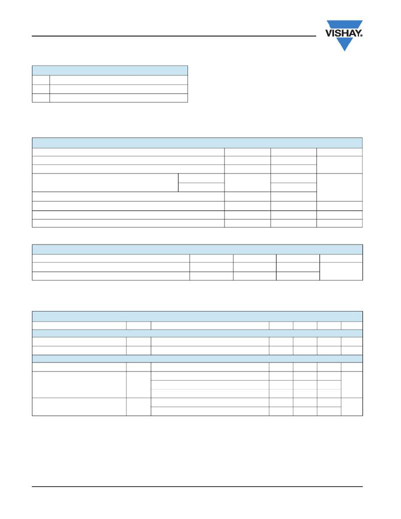
�R1� Pull-Up� Resistor�
�R2� Optional� Slew-Rate� Control�
�Typical� 10� k� ?� to� 1� m� ?� a�
�Typical� 0� to� 100� k� ?� a�
�The� Si1040X� is� ideally� suited� for� high-side� load� switching� in�
�portable� applications.� The� integrated� N-Channel� level-shift�
�device� saves� space� by� reducing� external� components.� The�
�slew� rate� is� set� externally� so� that� rise-times� can� be� tailored� to�
�C1�
�Optional� Slew-Rate� Control�
�Typical� 1000� pF�
�different� load� types.�
�Notes:�
�a.� Minimum� R1� value� should� be� at� least� 10� x� R2� to� ensure� Q1� turn-�
�on.�
�ABSOLUTE� MAXIMUM� RATINGS� (T� A� =� 25� °C,� unless� otherwise� noted)�
�Parameter�
�Input� Voltage�
�ON/OFF� Voltage�
�Symbol�
�V� IN�
�V� ON/OFF�
�Limit�
�8�
�8�
�Unit�
�V�
�Load� Current�
�Continuous� Intrinsic� Diode� Conduction� a�
�Continuous� a,� b�
�Pulsed� b,� c�
�I� L�
�I� S�
�±� 0.43�
�±� 1.0�
�-� 0.15�
�A�
�Maximum� Power� Dissipation� a�
�Operating� Junction� and� Storage� Temperature� Range�
�ESD� Rating,� MIL-STD-883D� Human� Body� Model� (100� pF,� 1500� ?� )�
�P� D�
�T� J� ,� T� stg�
�ESD�
�0.174�
�-� 55� to� 150�
�2�
�W�
�°C�
�kV�
�THERMAL� RESISTANCE� RATINGS�
�Parameter�
�Maximum� Junction-to-Ambient� (Continuous� Current)� a�
�Maximum� Junction-to-Foot� (Q2)�
�Symbol�
�R� thJA�
�R� thJC�
�Typical�
�600�
�450�
�Maximum�
�720�
�540�
�Unit�
�°C/� W�
�Notes:�
�a.� Surface� mounted� on� 1"� x� 1"� FR4� board.�
�SPECIFICATIONS� (T� J� =� 25� °C,� unless� otherwise� noted)�
�Parameter�
�Symbol�
�Test� Conditions�
�Min.�
�Typ.�
�Max.�
�Unit�
�OFF� Characteristics�
�Reverse� Leakage� Current�
�I� FL�
�V� IN� =� 8� V,� V� ON/OFF� =� 0� V�
�1�
�μ� A�
�Diode� Forward� Voltage�
�V� SD�
�I� S� =� -� 0.15� A�
�0.85�
�1.2�
�V�
�ON� Characteristics�
�Input� Voltage� Range�
�V� IN�
�V� ON/OFF� =� 1.5� V,� V� IN� =� 4.5� V,� I� D� =� 0.43� A�
�1.8�
�0.500�
�8�
�0.625�
�V�
�On-Resistance� (P-Channel)� at� 1� A�
�R� DS(on)�
�V� ON/OFF� =� 1.5� V,� V� IN� =� 2.5� V,� I� D� =� 0.36� A�
�0.710�
�0.890�
�?�
�V� ON/OFF� =� 1.5� V,� V� IN� =� 1.8� V,� I� D� =� 0.3� A�
�1.0�
�1.25�
�On-State� (P-Channel)� Drain� Current�
�I� D(on)�
�V� IN-OUT� ??� 0.2� V,� V� IN� =� 5� V,� V� ON/OFF� =� 1.5� V�
�V� IN-OUT� ??� 0.3� V,� V� IN� =� 3� V,� V� ON/OFF� =� 1.5� V�
�1�
�0.8�
�A�
�Notes:�
�a.� Surface� mounted� on� FR4� board.�
�b.� V� IN� =� 8� V,� V� ON/OFF� =� 8� V,� T� A� =� 25� °C.�
�c.� Pulse� test;� pulse� width� ?� 300� μ� s,� duty� cycle� ?� 2� %.�
�Stresses� beyond� those� listed� under� “Absolute� Maximum� Ratings”� may� cause� permanent� damage� to� the� device.� These� are� stress� ratings� only,� and� functional� operation�
�of� the� device� at� these� or� any� other� conditions� beyond� those� indicated� in� the� operational� sections� of� the� specifications� is� not� implied.� Exposure� to� absolute� maximum�
�rating� conditions� for� extended� periods� may� affect� device� reliability.�
�www.vishay.com�
�2�
�Document� Number:� 71809�
�S10-2544-Rev.� D,� 08-Nov-10�
�相关PDF资料 |
PDF描述 |
|---|---|
| SI1865DL-T1-GE3 | IC LOAD SW LVL SHIFT 1.2A SC70-6 |
| SI1867DL-T1-GE3 | IC LOAD SW LEVEL SHIFTER SC-70-6 |
| SI1869DH-T1-GE3 | IC LOAD SW LEVEL SHIFTER SC-70-6 |
| SI3460-E03-GM | IC POWER MANAGEMENT CTLR 11VQFN |
| SI3482-A01-GM | IC CTLR POE 24-48PORT PSE 24-QFN |
相关代理商/技术参数 |
参数描述 |
|---|---|
| SI104-100 | 制造商:未知厂家 制造商全称:未知厂家 功能描述:SMT Power Inductor |
| SI104-100K | 制造商:DELTA 制造商全称:Delta Electronics, Inc. 功能描述:SMT Power Inductor |
| SI104-101 | 制造商:未知厂家 制造商全称:未知厂家 功能描述:SMT Power Inductor |
| SI104-101K | 制造商:DELTA 制造商全称:Delta Electronics, Inc. 功能描述:SMT Power Inductor |
| SI104-120 | 制造商:未知厂家 制造商全称:未知厂家 功能描述:SMT Power Inductor |
发布紧急采购,3分钟左右您将得到回复。