- 您现在的位置:买卖IC网 > PDF目录8957 > SI5323-C-GM (Silicon Laboratories Inc)IC MULTIPLIER/ATTENUATOR 36-QFN PDF资料下载
参数资料
| 型号: | SI5323-C-GM |
| 厂商: | Silicon Laboratories Inc |
| 文件页数: | 22/40页 |
| 文件大小: | 0K |
| 描述: | IC MULTIPLIER/ATTENUATOR 36-QFN |
| 标准包装: | 490 |
| 系列: | DSPLL® |
| 类型: | 时钟乘法器 |
| PLL: | 是 |
| 输入: | 时钟 |
| 输出: | CML,CMOS,LVDS,LVPECL |
| 电路数: | 1 |
| 比率 - 输入:输出: | 2:2 |
| 差分 - 输入:输出: | 是/是 |
| 频率 - 最大: | 1.05GHz |
| 除法器/乘法器: | 无/是 |
| 电源电压: | 1.71 V ~ 3.63 V |
| 工作温度: | -40°C ~ 85°C |
| 安装类型: | 表面贴装 |
| 封装/外壳: | 36-VFQFN 裸露焊盘 |
| 供应商设备封装: | 36-QFN(6x6) |
| 包装: | 托盘 |
第1页第2页第3页第4页第5页第6页第7页第8页第9页第10页第11页第12页第13页第14页第15页第16页第17页第18页第19页第20页第21页当前第22页第23页第24页第25页第26页第27页第28页第29页第30页第31页第32页第33页第34页第35页第36页第37页第38页第39页第40页
Si5323
Rev. 1.0
29
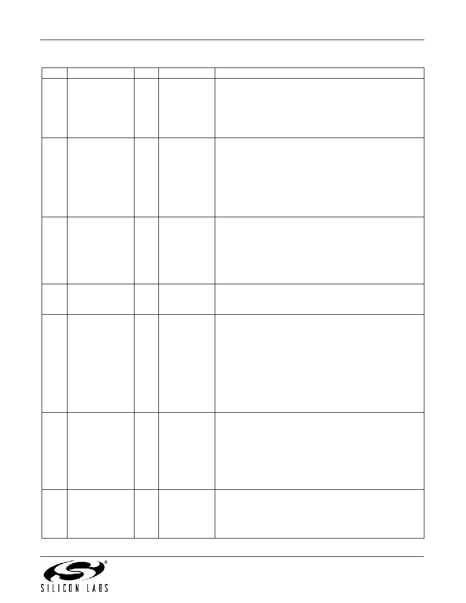
4C2B
O
LVCMOS
CKIN2 Loss of Signal.
Active high loss-of-signal indicator for CKIN2. Once
triggered, the alarm will remain active until CKIN2 is
validated.
0 = CKIN2 present
1 = LOS on CKIN2
5, 10,
32
VDD
Supply
Supply.
The device operates from a 1.8, 2.5, or 3.3 V supply. Bypass
capacitors should be associated with the following VDD pins:
5
0.1 F
10
0.1 F
32
0.1 F
A 1.0 F should also be placed as close to device as is
practical.
7
6
XB
XA
IAnalog
External Crystal or Reference Clock.
External crystal should be connected to these pins to use
internal oscillator based reference. Refer to Family
Reference Manual for interfacing to an external reference.
External reference must be from a high-quality clock source
(TCXO, OCXO). Frequency of crystal or external clock is set
by the RATE pins.
8, 31
GND
Supply
Ground.
Must be connected to system ground. Minimize the ground
path impedance for optimal performance of this device.
9
AUTOSEL
I
3-Level
Manual/Automatic Clock Selection.
Three level input that selects the method of input clock
selection to be used.
L = Manual
M = Automatic non-revertive
H = Automatic revertive
This pin has a weak pull-up and weak pull-down and defaults
to M.
Some designs may require an external resistor voltage
divider when driven by an active device that will tri-state.
11
15
RATE0
RATE1
I
3-Level
External Crystal or Reference Clock Rate.
Three level inputs that select the type and rate of external
crystal or reference clock to be applied to the XA/XB port.
Refer to the Family Reference Manual for settings. These
pins have both a weak pull-up and a weak pull-down and
default to M.
Some designs may require an external resistor voltage
divider when driven by an active device that will tri-state.
12
13
CKIN2+
CKIN2–
I
Clock Input 2.
Differential input clock. This input can also be driven with a
single-ended signal. Input frequency selected from a table of
values. The same frequency must be applied to CKIN1 and
CKIN2.
Table 12. Si5323 Pin Descriptions (Continued)
Pin #
Pin Name
I/O
Signal Level
Description
相关PDF资料 |
PDF描述 |
|---|---|
| VE-B41-MY-F3 | CONVERTER MOD DC/DC 12V 50W |
| VE-B1Z-MY-F1 | CONVERTER MOD DC/DC 2V 20W |
| VE-B1Z-MX-F4 | CONVERTER MOD DC/DC 2V 30W |
| VE-B1Z-MW-F1 | CONVERTER MOD DC/DC 2V 40W |
| VE-B1Y-MY-F4 | CONVERTER MOD DC/DC 3.3V 33W |
相关代理商/技术参数 |
参数描述 |
|---|---|
| SI5323-C-GMR | 功能描述:时钟合成器/抖动清除器 Pin-Ctrl Clk Xplier Jitter Attn 2In/Out RoHS:否 制造商:Skyworks Solutions, Inc. 输出端数量: 输出电平: 最大输出频率: 输入电平: 最大输入频率:6.1 GHz 电源电压-最大:3.3 V 电源电压-最小:2.7 V 封装 / 箱体:TSSOP-28 封装:Reel |
| SI5323-EVB | 制造商:Silicon Laboratories Inc 功能描述: |
| SI5324 | 制造商:SILABS 制造商全称:SILABS 功能描述:Pin-Controlled 1_710 MHz Jitter Cleaning Clock |
| Si5324A-C-GM | 功能描述:时钟合成器/抖动清除器 Prec.Clk Mult/Jitter Atten. 2kHz-1.4 GHz RoHS:否 制造商:Skyworks Solutions, Inc. 输出端数量: 输出电平: 最大输出频率: 输入电平: 最大输入频率:6.1 GHz 电源电压-最大:3.3 V 电源电压-最小:2.7 V 封装 / 箱体:TSSOP-28 封装:Reel |
| SI5324A-C-GMR | 功能描述:时钟合成器/抖动清除器 Lo Loop BW Clk Multi Jitter Attn 2In/Out RoHS:否 制造商:Skyworks Solutions, Inc. 输出端数量: 输出电平: 最大输出频率: 输入电平: 最大输入频率:6.1 GHz 电源电压-最大:3.3 V 电源电压-最小:2.7 V 封装 / 箱体:TSSOP-28 封装:Reel |
发布紧急采购,3分钟左右您将得到回复。