- 您现在的位置:买卖IC网 > PDF目录8718 > SI5330F-A00215-GM (Silicon Laboratories Inc)IC CLK BUFFER TRANSLA 1:8 24-QFN PDF资料下载
参数资料
| 型号: | SI5330F-A00215-GM |
| 厂商: | Silicon Laboratories Inc |
| 文件页数: | 20/20页 |
| 文件大小: | 0K |
| 描述: | IC CLK BUFFER TRANSLA 1:8 24-QFN |
| 标准包装: | 490 |
| 类型: | 扇出缓冲器(分配),变换器 |
| 电路数: | 1 |
| 比率 - 输入:输出: | 1:8 |
| 差分 - 输入:输出: | 无/无 |
| 输入: | CMOS,HSTL,LVTTL,SSTL |
| 输出: | CMOS |
| 频率 - 最大: | 200MHz |
| 电源电压: | 1.71 V ~ 3.63 V |
| 工作温度: | -40°C ~ 85°C |
| 安装类型: | 表面贴装 |
| 封装/外壳: | 24-VFQFN 裸露焊盘 |
| 供应商设备封装: | 24-QFN(4x4) |
| 包装: | 托盘 |
Si5330
Rev. 1.1
9
2. Functional Description
The Si5330 is a low-jitter, low-skew fanout buffer
optimized for high-performance PCB clock distribution
applications. The device produces four differential or
eight single-ended, low-jitter output clocks from a single
input clock. The input can accept either a single-ended
or a differential clock allowing the device to function as a
clock level translator.
2.1. VDD and VDDO Supplies
The core VDD and output VDDO supplies have separate
and independent supply pins allowing the core supply to
operate at a different voltage than the I/O voltage levels.
The VDD supply powers the core functions of the device,
which operates from 1.8, 2.5, or 3.3 V. Using a lower
supply voltage helps minimize the device’s power
consumption. The VDDO supply pins are used to set the
output signal levels and must be set at a voltage level
compatible with the output signal format.
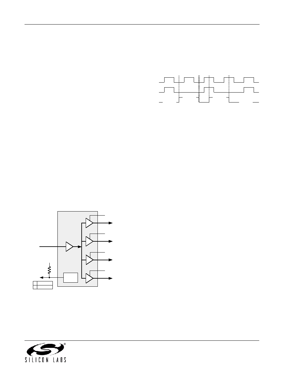
2.2. Loss Of Signal Indicator (LOS)
The input is monitored for a valid clock signal using an
LOS circuit that monitors input clock edges and
declares an LOS condition when signal edges are not
detected over a 1 to 5 μs observation period. The LOS
pin is asserted “low” when activity on the input clock pin
is present. A “high” level on the LOS pin indicates a loss
of signal (LOS). The LOS pin must be pulled to VDD as
shown in Figure 2.
Figure 2. LOS Indicator with External Pull-Up
2.3. Output Enable (OEB)
The output enable (OEB) pin allows disabling or
enabling of the outputs clocks (CLK0-CLK3). The output
enable is logically controlled to ensure that no glitches
or runt pulses are generated at the output as shown in
Figure 3. OEB Glitchless Operation
All outputs are enabled when the OEB pin is connected
to ground or below the VIL voltage for this pin.
Connecting the OEB pin to VDD or above the VIH level
will disable the outputs. Both VIL and VIH are specified
in Table 5. All outputs are forced to a logic “low” when
disabled. The OEB pin is 3.3 V tolerant.
2.4. Input Signals
The Si5330 can accept single-ended and differential
input clocks. See “AN408: Termination Options for Any-
Frequency, Any-Output Clock Generators and Clock
Buffers—Si5338, Si5334, Si5330” for details on
connecting a wide variety of signals to the Si5330
inputs.
2.5. Output Driver Formats
The Si5330 supports single-ended output formats of
CMOS, SSTL, and HSTL and differential formats of
LVDS, LVPECL, and HCSL. It is normally required that
the LVDS driver be dc-coupled to the 100
termination
at the receiver end. If your application requires an ac-
coupled 100
load, contact the applications team for
advice. See AN408 for additional information on the
terminations for these driver types.
2.6. Input and Output Terminations
See AN408 for detailed information.
3. Ordering the Si5330
The Si5330 can be ordered to meet the requirements of
the most commonly-used input and output signal types,
such as CMOS, SSTL, HSTL, LVPECL, LVDS, and
HSCL. See Figure 1, “Si5330 Functional Block
and Device Functionality,” on page 14 for specific
ordering information.
Si5330
Control
LOS
IN
VDDO0
CLK0
VDDO1
CLK1
VDDO2
CLK2
VDDO3
CLK3
VDD
1k
Valid Clock
No Clock
0
1
IN
CLKn
OEB
Enable
Disable
Enable
相关PDF资料 |
PDF描述 |
|---|---|
| SL23EP05SC-1 | IC BUFFER 220MHZ 5CH 3.3V 8SOIC |
| V24A36H400BG | CONVERTER MOD DC/DC 36V 400W |
| SL2309ZI-1 | IC BUFFER 140MHZ 9CH3.3V 16TSSOP |
| SL2309SI-1H | IC BUFFER 140MHZ 9CH 3.3V 16SOIC |
| V24A36H400BF3 | CONVERTER MOD DC/DC 36V 400W |
相关代理商/技术参数 |
参数描述 |
|---|---|
| SI5330F-A00215-GMR | 功能描述:时钟缓冲器 Sngl End In 2.5V out 1:8 ClkBuff 5-200MHz RoHS:否 制造商:Texas Instruments 输出端数量:5 最大输入频率:40 MHz 传播延迟(最大值): 电源电压-最大:3.45 V 电源电压-最小:2.375 V 最大功率耗散: 最大工作温度:+ 85 C 最小工作温度:- 40 C 封装 / 箱体:LLP-24 封装:Reel |
| Si5330F-A00216-GM | 功能描述:时钟缓冲器 Sngl-End 1.8 V CMOS 8-out, 5 to 200 MHz RoHS:否 制造商:Texas Instruments 输出端数量:5 最大输入频率:40 MHz 传播延迟(最大值): 电源电压-最大:3.45 V 电源电压-最小:2.375 V 最大功率耗散: 最大工作温度:+ 85 C 最小工作温度:- 40 C 封装 / 箱体:LLP-24 封装:Reel |
| SI5330F-A00216-GMR | 功能描述:时钟缓冲器 Sngl End In 1.8V out 1:8 ClkBuff 5-200MHz RoHS:否 制造商:Texas Instruments 输出端数量:5 最大输入频率:40 MHz 传播延迟(最大值): 电源电压-最大:3.45 V 电源电压-最小:2.375 V 最大功率耗散: 最大工作温度:+ 85 C 最小工作温度:- 40 C 封装 / 箱体:LLP-24 封装:Reel |
| Si5330F-B00214-GM | 功能描述:时钟缓冲器 Sngl-end input CMOS 5 - 200 MHz RoHS:否 制造商:Texas Instruments 输出端数量:5 最大输入频率:40 MHz 传播延迟(最大值): 电源电压-最大:3.45 V 电源电压-最小:2.375 V 最大功率耗散: 最大工作温度:+ 85 C 最小工作温度:- 40 C 封装 / 箱体:LLP-24 封装:Reel |
| SI5330F-B00214-GMR | 功能描述:时钟缓冲器 Sngl End In 3.3V out 1:8 ClkBuff 5-200MHz RoHS:否 制造商:Texas Instruments 输出端数量:5 最大输入频率:40 MHz 传播延迟(最大值): 电源电压-最大:3.45 V 电源电压-最小:2.375 V 最大功率耗散: 最大工作温度:+ 85 C 最小工作温度:- 40 C 封装 / 箱体:LLP-24 封装:Reel |
发布紧急采购,3分钟左右您将得到回复。