- 您现在的位置:买卖IC网 > PDF目录8718 > SI5330F-A00215-GM (Silicon Laboratories Inc)IC CLK BUFFER TRANSLA 1:8 24-QFN PDF资料下载
参数资料
| 型号: | SI5330F-A00215-GM |
| 厂商: | Silicon Laboratories Inc |
| 文件页数: | 3/20页 |
| 文件大小: | 0K |
| 描述: | IC CLK BUFFER TRANSLA 1:8 24-QFN |
| 标准包装: | 490 |
| 类型: | 扇出缓冲器(分配),变换器 |
| 电路数: | 1 |
| 比率 - 输入:输出: | 1:8 |
| 差分 - 输入:输出: | 无/无 |
| 输入: | CMOS,HSTL,LVTTL,SSTL |
| 输出: | CMOS |
| 频率 - 最大: | 200MHz |
| 电源电压: | 1.71 V ~ 3.63 V |
| 工作温度: | -40°C ~ 85°C |
| 安装类型: | 表面贴装 |
| 封装/外壳: | 24-VFQFN 裸露焊盘 |
| 供应商设备封装: | 24-QFN(4x4) |
| 包装: | 托盘 |
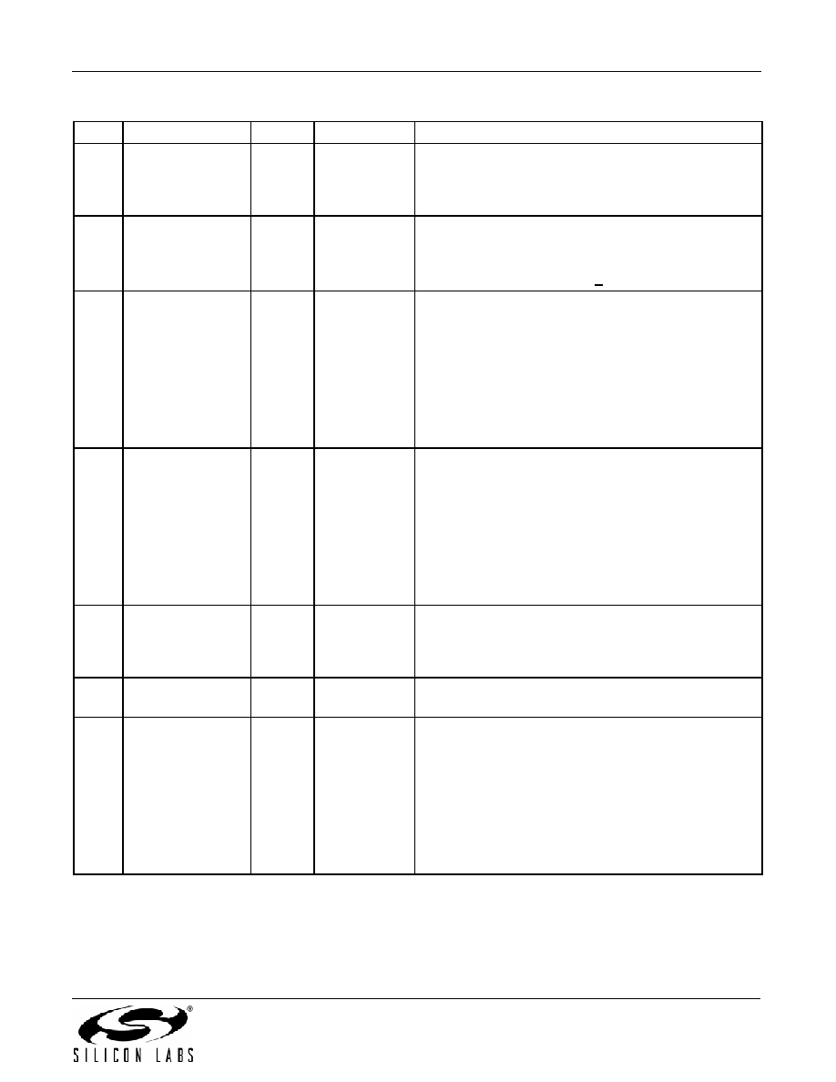
Si5330
Rev. 1.1
11
7
VDD
Supply
Core Supply Voltage.
The device operates from a 1.8, 2.5, or 3.3 V supply. A
0.1 F bypass capacitor should be located very close to
this pin.
8
LOS
O
Open Drain
Loss of Signal Indicator.
0 = CLKIN present.
1 = Loss of signal (LOS).
This pin requires an external
1kpull-up resistor.
9
CLK3B
O
Multi
Si5330A/B/C/K/L/M Differential Output Devices.
This is the negative side of the differential CLK3 output.
Refer to AN408 for interfacing and termination details.
Leave unconnected when not in use.
Si5330F/G/H/J Single-Ended Output Devices.
This is one of the single-ended CLK3 outputs. Both
CLK3A and CLK3B single-ended outputs are in phase.
Refer to AN408 for interfacing and termination details.
Leave unconnected when not is use.
10
CLK3A
O
Multi
Si5330A/B/C/K/L/M Differential Devices.
This is the positive side of the differential CLK3 output.
Refer to AN408 for interfacing and termination details.
Leave unconnected when not in use.
Si5330F/G/H/J Single-Ended Devices.
This is one of the single-ended CLK3 outputs. Both
CLK3A and CLK3B single-ended outputs are in phase.
Refer to AN408 for interfacing and termination details.
Leave unconnected when not is use.
11
VDDO3
VDD
Supply
Output Clock Supply Voltage.
Supply voltage for CLK3A/B. Use a 0.1 F bypass cap
as close as possible to this pin. If CLK3 is not used, this
pin must be tied to VDD (pin 7 and/or pin 24).
12
RSVD_GND
Ground.
Must be connected to system ground.
13
CLK2B
O
Multi
Si5330A/B/C/K/L/M Differential Output Devices.
This is the negative side of the differential CLK2 output.
Refer to AN408 for interfacing and termination details.
Leave unconnected when not in use.
Si5330F/G/H/J Single-Ended Output Devices.
This is one of the single-ended CLK2 outputs. Both
CLK2A and CLK2B single-ended outputs are in phase.
Refer to AN408 for interfacing and termination details.
Leave unconnected when not is use.
Table 10. Si5330 Pin Descriptions (Continued)
Pin #
Pin Name
I/O
Signal Type
Description
相关PDF资料 |
PDF描述 |
|---|---|
| SL23EP05SC-1 | IC BUFFER 220MHZ 5CH 3.3V 8SOIC |
| V24A36H400BG | CONVERTER MOD DC/DC 36V 400W |
| SL2309ZI-1 | IC BUFFER 140MHZ 9CH3.3V 16TSSOP |
| SL2309SI-1H | IC BUFFER 140MHZ 9CH 3.3V 16SOIC |
| V24A36H400BF3 | CONVERTER MOD DC/DC 36V 400W |
相关代理商/技术参数 |
参数描述 |
|---|---|
| SI5330F-A00215-GMR | 功能描述:时钟缓冲器 Sngl End In 2.5V out 1:8 ClkBuff 5-200MHz RoHS:否 制造商:Texas Instruments 输出端数量:5 最大输入频率:40 MHz 传播延迟(最大值): 电源电压-最大:3.45 V 电源电压-最小:2.375 V 最大功率耗散: 最大工作温度:+ 85 C 最小工作温度:- 40 C 封装 / 箱体:LLP-24 封装:Reel |
| Si5330F-A00216-GM | 功能描述:时钟缓冲器 Sngl-End 1.8 V CMOS 8-out, 5 to 200 MHz RoHS:否 制造商:Texas Instruments 输出端数量:5 最大输入频率:40 MHz 传播延迟(最大值): 电源电压-最大:3.45 V 电源电压-最小:2.375 V 最大功率耗散: 最大工作温度:+ 85 C 最小工作温度:- 40 C 封装 / 箱体:LLP-24 封装:Reel |
| SI5330F-A00216-GMR | 功能描述:时钟缓冲器 Sngl End In 1.8V out 1:8 ClkBuff 5-200MHz RoHS:否 制造商:Texas Instruments 输出端数量:5 最大输入频率:40 MHz 传播延迟(最大值): 电源电压-最大:3.45 V 电源电压-最小:2.375 V 最大功率耗散: 最大工作温度:+ 85 C 最小工作温度:- 40 C 封装 / 箱体:LLP-24 封装:Reel |
| Si5330F-B00214-GM | 功能描述:时钟缓冲器 Sngl-end input CMOS 5 - 200 MHz RoHS:否 制造商:Texas Instruments 输出端数量:5 最大输入频率:40 MHz 传播延迟(最大值): 电源电压-最大:3.45 V 电源电压-最小:2.375 V 最大功率耗散: 最大工作温度:+ 85 C 最小工作温度:- 40 C 封装 / 箱体:LLP-24 封装:Reel |
| SI5330F-B00214-GMR | 功能描述:时钟缓冲器 Sngl End In 3.3V out 1:8 ClkBuff 5-200MHz RoHS:否 制造商:Texas Instruments 输出端数量:5 最大输入频率:40 MHz 传播延迟(最大值): 电源电压-最大:3.45 V 电源电压-最小:2.375 V 最大功率耗散: 最大工作温度:+ 85 C 最小工作温度:- 40 C 封装 / 箱体:LLP-24 封装:Reel |
发布紧急采购,3分钟左右您将得到回复。