- 您现在的位置:买卖IC网 > PDF目录8953 > SI5369B-C-GQ (Silicon Laboratories Inc)IC CLK MULT JITTER ATTEN 100TQFP PDF资料下载
参数资料
| 型号: | SI5369B-C-GQ |
| 厂商: | Silicon Laboratories Inc |
| 文件页数: | 24/84页 |
| 文件大小: | 0K |
| 描述: | IC CLK MULT JITTER ATTEN 100TQFP |
| 标准包装: | 90 |
| 系列: | DSPLL® |
| 类型: | * |
| PLL: | 是 |
| 输入: | LVCMOS |
| 输出: | CML,CMOS,LVDS,LVPECL |
| 电路数: | 1 |
| 比率 - 输入:输出: | 4:5 |
| 差分 - 输入:输出: | 是/是 |
| 频率 - 最大: | 808MHz |
| 除法器/乘法器: | 是/是 |
| 电源电压: | 1.71 V ~ 3.63 V |
| 工作温度: | -40°C ~ 85°C |
| 安装类型: | 表面贴装 |
| 封装/外壳: | 100-TQFP |
| 供应商设备封装: | 100-TQFP(14x14) |
| 包装: | 托盘 |
第1页第2页第3页第4页第5页第6页第7页第8页第9页第10页第11页第12页第13页第14页第15页第16页第17页第18页第19页第20页第21页第22页第23页当前第24页第25页第26页第27页第28页第29页第30页第31页第32页第33页第34页第35页第36页第37页第38页第39页第40页第41页第42页第43页第44页第45页第46页第47页第48页第49页第50页第51页第52页第53页第54页第55页第56页第57页第58页第59页第60页第61页第62页第63页第64页第65页第66页第67页第68页第69页第70页第71页第72页第73页第74页第75页第76页第77页第78页第79页第80页第81页第82页第83页第84页
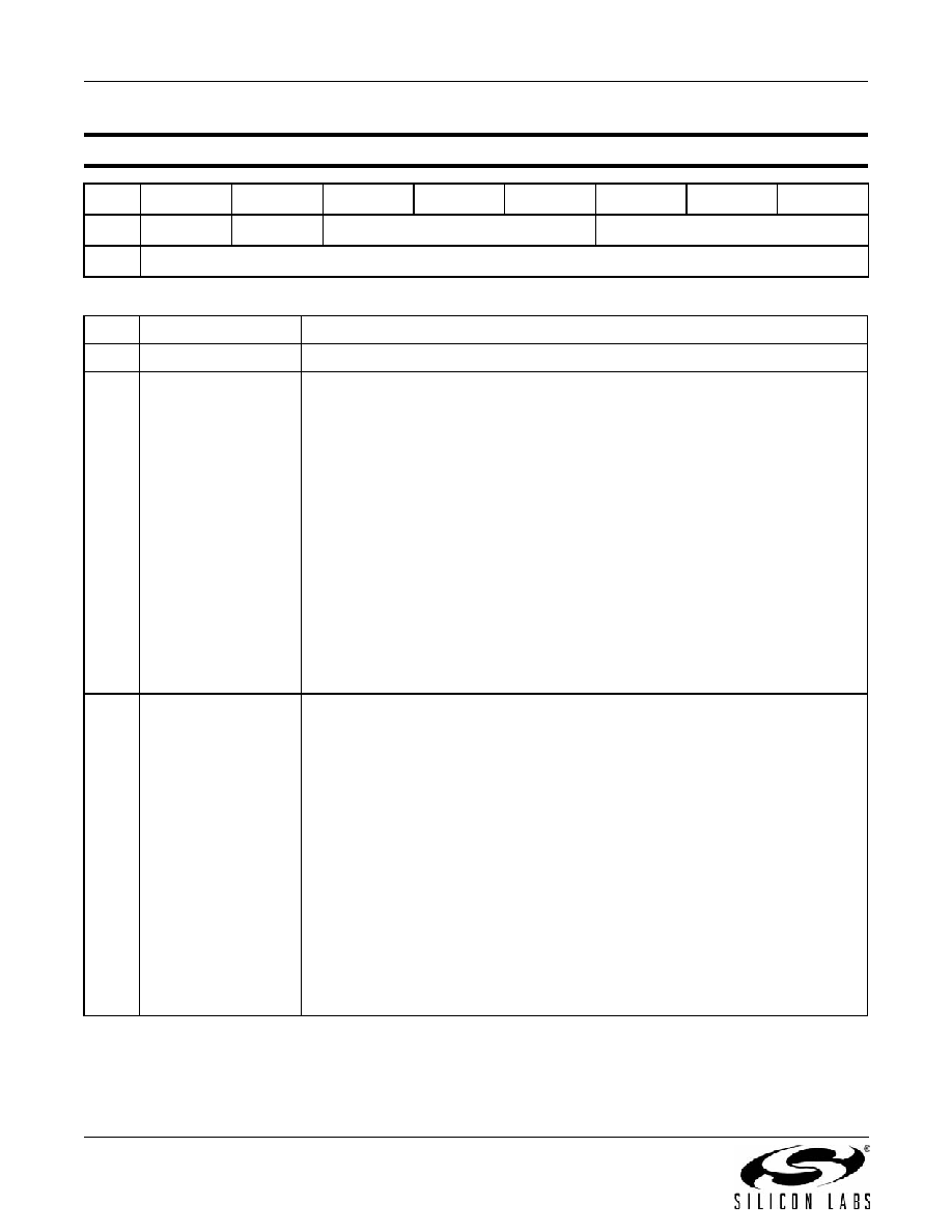
Si5369
30
Rev. 1.0
Reset value = 0010 1100
Register 6.
Bit
D7
D6
D5D4D3
D2D1
D0
Name
SFOUT4_REG [2:0]
SFOUT3_REG [2:0]
Type
RR
R/W
Bit
Name
Function
7:6
Reserved
5:3
SFOUT4_REG [2:0]
SFOUT4_REG [2:0].
Controls output signal format and disable for CKOUT4 output buffer. The LVPECL
and CMOS output formats draw more current than either LVDS or CML; however,
there are restrictions in the allowed output format pin settings so that the maxi-
mum power dissipation for the TQFP devices is limited when they are operated at
3.3 V. When there are four enabled LVPECL or CMOS outputs, the fifth output
must be disabled. When there are five enabled outputs, there can be no more
than three outputs that are either LVPECL or CMOS.
000: Reserved
001: Disable
010: CMOS
011: Low swing LVDS
100: Reserved
101: LVPECL
110: CML
111: LVDS
2:0
SFOUT3_REG [2:0]
SFOUT3_REG [2:0].
Controls output signal format and disable for CKOUT3 output buffer. The LVPECL
and CMOS output formats draw more current than either LVDS or CML; however,
there are restrictions in the allowed output format pin settings so that the maxi-
mum power dissipation for the TQFP devices is limited when they are operated at
3.3 V. When there are four enabled LVPECL or CMOS outputs, the fifth output
must be disabled. When there are five enabled outputs, there can be no more
than three outputs that are either LVPECL or CMOS.
000: Reserved
001: Disable
010: CMOS
011: Low swing LVDS
100: Reserved
101: LVPECL
110: CML
111: LVDS
相关PDF资料 |
PDF描述 |
|---|---|
| VE-210-MY-F1 | CONVERTER MOD DC/DC 5V 50W |
| VE-B5N-MY-F3 | CONVERTER MOD DC/DC 18.5V 50W |
| VE-20L-MY-F4 | CONVERTER MOD DC/DC 28V 50W |
| VE-20L-MY-F2 | CONVERTER MOD DC/DC 28V 50W |
| VE-20L-MY-F1 | CONVERTER MOD DC/DC 28V 50W |
相关代理商/技术参数 |
参数描述 |
|---|---|
| SI5369B-C-GQR | 功能描述:时钟发生器及支持产品 Lo Loop BW Clk Multi Jitter Attn 4In/5Out RoHS:否 制造商:Silicon Labs 类型:Clock Generators 最大输入频率:14.318 MHz 最大输出频率:166 MHz 输出端数量:16 占空比 - 最大:55 % 工作电源电压:3.3 V 工作电源电流:1 mA 最大工作温度:+ 85 C 安装风格:SMD/SMT 封装 / 箱体:QFN-56 |
| Si5369C-C-GQ | 功能描述:时钟发生器及支持产品 LW LOOP BW AR CLK MULT/JITTER 4IN 5OUT RoHS:否 制造商:Silicon Labs 类型:Clock Generators 最大输入频率:14.318 MHz 最大输出频率:166 MHz 输出端数量:16 占空比 - 最大:55 % 工作电源电压:3.3 V 工作电源电流:1 mA 最大工作温度:+ 85 C 安装风格:SMD/SMT 封装 / 箱体:QFN-56 |
| SI5369C-C-GQR | 功能描述:时钟发生器及支持产品 Lo Loop BW Clk Multi Jitter Attn 4In/5Out RoHS:否 制造商:Silicon Labs 类型:Clock Generators 最大输入频率:14.318 MHz 最大输出频率:166 MHz 输出端数量:16 占空比 - 最大:55 % 工作电源电压:3.3 V 工作电源电流:1 mA 最大工作温度:+ 85 C 安装风格:SMD/SMT 封装 / 箱体:QFN-56 |
| Si5369D-C-GQ | 功能描述:时钟发生器及支持产品 LW LOOP BW AR CLK MULT/JITTER 4IN 5OUT RoHS:否 制造商:Silicon Labs 类型:Clock Generators 最大输入频率:14.318 MHz 最大输出频率:166 MHz 输出端数量:16 占空比 - 最大:55 % 工作电源电压:3.3 V 工作电源电流:1 mA 最大工作温度:+ 85 C 安装风格:SMD/SMT 封装 / 箱体:QFN-56 |
| SI5369D-C-GQR | 功能描述:时钟发生器及支持产品 Lo Loop BW Clk Multi Jitter Attn 4In/5Out RoHS:否 制造商:Silicon Labs 类型:Clock Generators 最大输入频率:14.318 MHz 最大输出频率:166 MHz 输出端数量:16 占空比 - 最大:55 % 工作电源电压:3.3 V 工作电源电流:1 mA 最大工作温度:+ 85 C 安装风格:SMD/SMT 封装 / 箱体:QFN-56 |
发布紧急采购,3分钟左右您将得到回复。