- 您现在的位置:买卖IC网 > PDF目录8953 > SI5369B-C-GQ (Silicon Laboratories Inc)IC CLK MULT JITTER ATTEN 100TQFP PDF资料下载
参数资料
| 型号: | SI5369B-C-GQ |
| 厂商: | Silicon Laboratories Inc |
| 文件页数: | 74/84页 |
| 文件大小: | 0K |
| 描述: | IC CLK MULT JITTER ATTEN 100TQFP |
| 标准包装: | 90 |
| 系列: | DSPLL® |
| 类型: | * |
| PLL: | 是 |
| 输入: | LVCMOS |
| 输出: | CML,CMOS,LVDS,LVPECL |
| 电路数: | 1 |
| 比率 - 输入:输出: | 4:5 |
| 差分 - 输入:输出: | 是/是 |
| 频率 - 最大: | 808MHz |
| 除法器/乘法器: | 是/是 |
| 电源电压: | 1.71 V ~ 3.63 V |
| 工作温度: | -40°C ~ 85°C |
| 安装类型: | 表面贴装 |
| 封装/外壳: | 100-TQFP |
| 供应商设备封装: | 100-TQFP(14x14) |
| 包装: | 托盘 |
第1页第2页第3页第4页第5页第6页第7页第8页第9页第10页第11页第12页第13页第14页第15页第16页第17页第18页第19页第20页第21页第22页第23页第24页第25页第26页第27页第28页第29页第30页第31页第32页第33页第34页第35页第36页第37页第38页第39页第40页第41页第42页第43页第44页第45页第46页第47页第48页第49页第50页第51页第52页第53页第54页第55页第56页第57页第58页第59页第60页第61页第62页第63页第64页第65页第66页第67页第68页第69页第70页第71页第72页第73页当前第74页第75页第76页第77页第78页第79页第80页第81页第82页第83页第84页
Si5369
76
Rev. 1.0
49
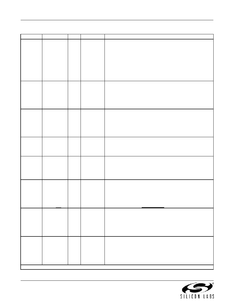
LOL
O
LVCMOS
PLL Loss of Lock Indicator.
This pin functions as the active high PLL loss of lock indicator if
the LOL_PIN register bit is set to one.
0 = PLL locked.
1 = PLL unlocked.
If LOL_PIN = 0, this pin will tristate.
Active polarity is controlled by the LOL_POL bit. The PLL lock
status will always be reflected in the LOL_INT read only register
bit.
58
C1A
O
LVCMOS
CKIN1 Active Clock Indicator.
This pin serves as the CKIN1 active clock indicator. The
CK1_ACTV_REG bit always reflects the active clock status for
CKIN1. If CK1_ACTV_PIN = 1, this status will also be reflected
on the C1A pin with active polarity controlled by the CK_ACT-
V_POL bit. If CK1_ACTV_PIN = 0, this output tristates.
59
C2A
O
LVCMOS
CKIN2 Active Clock Indicator.
This pin serves as the CKIN2 active clock indicator. The
CK2_ACTV_REG bit always reflects the active clock status for
CKIN_2. If CK2_ACTV_PIN = 1, this status will also be reflected
on the C2A pin with active polarity controlled by the CK_ACT-
V_POL bit. If CK2_ACTV_PIN = 0, this output tristates.
60
SCL
I
LVCMOS
Serial Clock.
This pin functions as the serial port clock input for both SPI and
I2C modes.
This pin has a weak pull-down.
61
SDA_SDO
I/O
LVCMOS
Serial Data.
In I2C microprocessor control mode (CMODE = 0), this pin func-
tions as the bidirectional serial data port. In SPI microprocessor
control mode (CMODE = 1), this pin functions as the serial data
output.
68
69
A0
A1
ILVCMOS
Serial Port Address.
In I2C microprocessor control mode (CMODE = 0), these pins
function as hardware controlled address bits. The I2C address
is 1101 [A2] [A1] [A0]. In SPI microprocessor control mode
(CMODE = 1), these pins are ignored.
This pin has a weak pull-down.
70
A2_SS
ILVCMOS
Serial Port Address/Slave Select.
In I2C microprocessor control mode (CMODE = 0), this pin func-
tions as a hardware controlled address bit [A2].
In SPI microprocessor control mode (CMODE = 1), this pin
functions as the slave select input.
This pin has a weak pull-down.
71
SDI
I
LVCMOS
Serial Data In.
In SPI microprocessor control mode (CMODE = 1), this pin
functions as the serial data input.
In I2C microprocessor control mode (CMODE = 0), this pin is
ignored.
This pin has a weak pull-down.
Table 10. Si5369 Pin Descriptions (Continued)
Pin #
Pin Name
I/O
Signal Level
Description
Note: Internal register names are indicated by underlined italics, e.g., INT_PIN. See Si5369 Register Map.
相关PDF资料 |
PDF描述 |
|---|---|
| VE-210-MY-F1 | CONVERTER MOD DC/DC 5V 50W |
| VE-B5N-MY-F3 | CONVERTER MOD DC/DC 18.5V 50W |
| VE-20L-MY-F4 | CONVERTER MOD DC/DC 28V 50W |
| VE-20L-MY-F2 | CONVERTER MOD DC/DC 28V 50W |
| VE-20L-MY-F1 | CONVERTER MOD DC/DC 28V 50W |
相关代理商/技术参数 |
参数描述 |
|---|---|
| SI5369B-C-GQR | 功能描述:时钟发生器及支持产品 Lo Loop BW Clk Multi Jitter Attn 4In/5Out RoHS:否 制造商:Silicon Labs 类型:Clock Generators 最大输入频率:14.318 MHz 最大输出频率:166 MHz 输出端数量:16 占空比 - 最大:55 % 工作电源电压:3.3 V 工作电源电流:1 mA 最大工作温度:+ 85 C 安装风格:SMD/SMT 封装 / 箱体:QFN-56 |
| Si5369C-C-GQ | 功能描述:时钟发生器及支持产品 LW LOOP BW AR CLK MULT/JITTER 4IN 5OUT RoHS:否 制造商:Silicon Labs 类型:Clock Generators 最大输入频率:14.318 MHz 最大输出频率:166 MHz 输出端数量:16 占空比 - 最大:55 % 工作电源电压:3.3 V 工作电源电流:1 mA 最大工作温度:+ 85 C 安装风格:SMD/SMT 封装 / 箱体:QFN-56 |
| SI5369C-C-GQR | 功能描述:时钟发生器及支持产品 Lo Loop BW Clk Multi Jitter Attn 4In/5Out RoHS:否 制造商:Silicon Labs 类型:Clock Generators 最大输入频率:14.318 MHz 最大输出频率:166 MHz 输出端数量:16 占空比 - 最大:55 % 工作电源电压:3.3 V 工作电源电流:1 mA 最大工作温度:+ 85 C 安装风格:SMD/SMT 封装 / 箱体:QFN-56 |
| Si5369D-C-GQ | 功能描述:时钟发生器及支持产品 LW LOOP BW AR CLK MULT/JITTER 4IN 5OUT RoHS:否 制造商:Silicon Labs 类型:Clock Generators 最大输入频率:14.318 MHz 最大输出频率:166 MHz 输出端数量:16 占空比 - 最大:55 % 工作电源电压:3.3 V 工作电源电流:1 mA 最大工作温度:+ 85 C 安装风格:SMD/SMT 封装 / 箱体:QFN-56 |
| SI5369D-C-GQR | 功能描述:时钟发生器及支持产品 Lo Loop BW Clk Multi Jitter Attn 4In/5Out RoHS:否 制造商:Silicon Labs 类型:Clock Generators 最大输入频率:14.318 MHz 最大输出频率:166 MHz 输出端数量:16 占空比 - 最大:55 % 工作电源电压:3.3 V 工作电源电流:1 mA 最大工作温度:+ 85 C 安装风格:SMD/SMT 封装 / 箱体:QFN-56 |
发布紧急采购,3分钟左右您将得到回复。