- 您现在的位置:买卖IC网 > Datasheet目录512 > SI5933DC-T1-GE3 (Vishay Siliconix)MOSFET DUAL P-CH 20V 2.7A 1206-8 Datasheet资料下载
参数资料
| 型号: | SI5933DC-T1-GE3 |
| 厂商: | Vishay Siliconix |
| 文件页数: | 2/9页 |
| 文件大小: | 0K |
| 描述: | MOSFET DUAL P-CH 20V 2.7A 1206-8 |
| 标准包装: | 3,000 |
| 系列: | TrenchFET® |
| FET 型: | 2 个 P 沟道(双) |
| FET 特点: | 逻辑电平门 |
| 漏极至源极电压(Vdss): | 20V |
| 电流 - 连续漏极(Id) @ 25° C: | 2.7A |
| 开态Rds(最大)@ Id, Vgs @ 25° C: | 110 毫欧 @ 2.7A,4.5V |
| Id 时的 Vgs(th)(最大): | 1V @ 250µA |
| 闸电荷(Qg) @ Vgs: | 7.7nC @ 4.5V |
| 功率 - 最大: | 1.1W |
| 安装类型: | 表面贴装 |
| 封装/外壳: | 8-SMD,扁平引线 |
| 供应商设备封装: | 1206-8 ChipFET? |
| 包装: | 带卷 (TR) |
�� �
�
�Si5933DC�
�Vishay� Siliconix�
�SPECIFICATIONS� T� J� =� 25� °C,� unless� otherwise� noted�
�Parameter�
�Symbol�
�Test� Conditions�
�Min.�
�Typ.�
�Max.�
�Unit�
�Static�
�Gate� Threshold� Voltage�
�V� GS(th)�
�V� DS� =� V� GS� ,� I� D� =� -� 250� μA�
�-� 0.45�
�-� 1.0�
�V�
�Gate-Body� Leakage�
�Zero� Gate� Voltage� Drain� Current�
�On-State� Drain� Current� a�
�I� GSS�
�I� DSS�
�I� D(on)�
�V� DS� =� 0� V,� V� GS� =� ±� 8� V�
�V� DS� =� -� 20� V,� V� GS� =� 0� V�
�V� DS� =� -� 20� V,� V� GS� =� 0� V,� T� J� =� 85� °C�
�V� DS� ≤� -� 5� V,� V� GS� =� -� 4.5� V�
�V� GS� =� -� 4.5� V,� I� D� =� -� 2.7� A�
�-� 10�
�0.095�
�±� 100�
�-1�
�-5�
�0.110�
�nA�
�μA�
�A�
�Drain-Source� On-State� Resistance� a�
�R� DS(on)�
�V� GS� =� -� 2.5� V,� I� D� =� -� 2.2� A�
�0.137�
�0.160�
�Ω�
�V� GS� =� -� 1.8� V,� I� D� =� -� 1� A�
�0.205�
�0.240�
�Forward� Transconductance� a�
�g� fs�
�V� DS� =� -� 10� V,� I� D� =� -� 2.7� A�
�7�
�S�
�Diode� Forward� Voltage�
�a�
�V� SD�
�I� S� =� -� 0.9� A,� V� GS� =� 0� V�
�-� 0.8�
�-� 1.2�
�V�
�Dynamic� b�
�Total� Gate� Charge�
�Q� g�
�5.1�
�7.7�
�Gate-Source� Charge�
�Gate-Drain� Charge�
�Turn-On� Delay� Time�
�Q� gs�
�Q� gd�
�t� d(on)�
�V� DS� =� -� 10� V,� V� GS� =� -� 4.5� V,� I� D� =� -� 2.7� A�
�1.2�
�1.0�
�16�
�25�
�nC�
�Rise� Time�
�Turn-Off� Delay� Time�
�Fall� Time�
�Source-Drain� Reverse� Recovery� Time�
�t� r�
�t� d(off)�
�t� f�
�t� rr�
�V� DD� =� -� 10� V,� R� L� =� 10� Ω�
�I� D� ?� -� 1� A,� V� GEN� =� -� 4.5� V,� R� g� =� 6� Ω�
�I� F� =� -� 0.9� A,� dI/dt� =� 100� A/μs�
�30�
�30�
�27�
�20�
�45�
�45�
�40�
�40�
�ns�
�Notes:�
�a.� Pulse� test;� pulse� width� ≤� 300� μs,� duty� cycle� ≤� 2� %.�
�b.� Guaranteed� by� design,� not� subject� to� production� testing.�
�Stresses� beyond� those� listed� under� “Absolute� Maximum� Ratings”� may� cause� permanent� damage� to� the� device.� These� are� stress� ratings� only,� and� functional� operation�
�of� the� device� at� these� or� any� other� conditions� beyond� those� indicated� in� the� operational� sections� of� the� specifications� is� not� implied.� Exposure� to� absolute� maximum�
�rating� conditions� for� extended� periods� may� affect� device� reliability.�
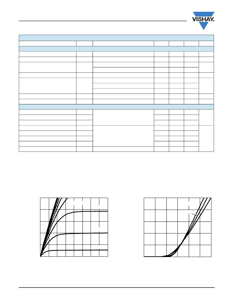
�TYPICAL� CHARACTERISTICS� 25� °C,� unless� otherwise� noted�
�10�
�V� GS� = 5 V thru 3 V�
�10�
�T� C� = - 55 °C�
�8�
�2.5� V�
�8�
�25 °C�
�125� °C�
�6�
�4�
�2V�
�6�
�4�
�2�
�0�
�1.5� V�
�2�
�0�
�0.0�
�0.5�
�1.0�
�1.5�
�2.0�
�2.5�
�3.0�
�3.5�
�4.0�
�0.0�
�0.5�
�1.0�
�1.5�
�2.0�
�2.5�
�3.0�
�www.vishay.com�
�2�
�V� DS� -� Drain-to-Source� Voltage� (V)�
�Output� Characteristics�
�V� GS� -� Gate-to-Source� Voltage� (V)�
�Transfer� Characteristics�
�Document� Number:� 71238�
�S10-0936-Rev.� E,� 19-Apr-10�
�相关PDF资料 |
PDF描述 |
|---|---|
| SI5935DC-T1-GE3 | MOSFET DUAL P-CH 20V 1206-8 |
| SI5943DU-T1-GE3 | MOSFET DUAL P-CH 12V 6A 8PWRPAK |
| SI5975DC-T1-GE3 | MOSFET 2P-CH 12V 3.1A CHIPFET |
| SI5980DU-T1-GE3 | MOSFET N-CH 100V PPAK CHIPFET |
| SI6404DQ-T1-GE3 | MOSFET N-CH 30V 8.6A 8TSSOP |
相关代理商/技术参数 |
参数描述 |
|---|---|
| SI5935CDC | 制造商:VISHAY 制造商全称:Vishay Siliconix 功能描述:Dual P-Channel 20-V (D-S) MOSFET |
| SI5935CDC-T1-E3 | 功能描述:MOSFET 20V 4.0A 3.1W 100mohm @ 4.5V RoHS:否 制造商:STMicroelectronics 晶体管极性:N-Channel 汲极/源极击穿电压:650 V 闸/源击穿电压:25 V 漏极连续电流:130 A 电阻汲极/源极 RDS(导通):0.014 Ohms 配置:Single 最大工作温度: 安装风格:Through Hole 封装 / 箱体:Max247 封装:Tube |
| SI5935CDC-T1-GE3 | 功能描述:MOSFET 20V 4A 3.1W RoHS:否 制造商:STMicroelectronics 晶体管极性:N-Channel 汲极/源极击穿电压:650 V 闸/源击穿电压:25 V 漏极连续电流:130 A 电阻汲极/源极 RDS(导通):0.014 Ohms 配置:Single 最大工作温度: 安装风格:Through Hole 封装 / 箱体:Max247 封装:Tube |
| SI5935DC | 制造商:VISHAY 制造商全称:Vishay Siliconix 功能描述:Dual P-Channel 1.8-V (G-S) MOSFET |
| SI5935DC-T1 | 制造商:VISHAY 制造商全称:Vishay Siliconix 功能描述:Dual P-Channel 1.8-V (G-S) MOSFET |
发布紧急采购,3分钟左右您将得到回复。