- 您现在的位置:买卖IC网 > Datasheet目录512 > SI5933DC-T1-GE3 (Vishay Siliconix)MOSFET DUAL P-CH 20V 2.7A 1206-8 Datasheet资料下载
参数资料
| 型号: | SI5933DC-T1-GE3 |
| 厂商: | Vishay Siliconix |
| 文件页数: | 6/9页 |
| 文件大小: | 0K |
| 描述: | MOSFET DUAL P-CH 20V 2.7A 1206-8 |
| 标准包装: | 3,000 |
| 系列: | TrenchFET® |
| FET 型: | 2 个 P 沟道(双) |
| FET 特点: | 逻辑电平门 |
| 漏极至源极电压(Vdss): | 20V |
| 电流 - 连续漏极(Id) @ 25° C: | 2.7A |
| 开态Rds(最大)@ Id, Vgs @ 25° C: | 110 毫欧 @ 2.7A,4.5V |
| Id 时的 Vgs(th)(最大): | 1V @ 250µA |
| 闸电荷(Qg) @ Vgs: | 7.7nC @ 4.5V |
| 功率 - 最大: | 1.1W |
| 安装类型: | 表面贴装 |
| 封装/外壳: | 8-SMD,扁平引线 |
| 供应商设备封装: | 1206-8 ChipFET? |
| 包装: | 带卷 (TR) |
�� �
�
�AN812�
�Vishay� Siliconix�
�Dual-Channel� 1206-8� ChipFET� r� Power� MOSFET� Recommended�
�Pad� Pattern� and� Thermal� Performance�
�INTRODUCTION�
�New� Vishay� Siliconix� ChipFETs� in� the� leadless� 1206-8�
�package� feature� the� same� outline� as� popular� 1206-8� resistors�
�and� capacitors� but� provide� all� the� performance� of� true� power�
�semiconductor� devices.� The� 1206-8� ChipFET� has� the� same�
�footprint� as� the� body� of� the� LITTLE� FOOT� R� TSOP-6,� and� can�
�be� thought� of� as� a� leadless� TSOP-6� for� purposes� of� visualizing�
�board� area,� but� its� thermal� performance� bears� comparison�
�with� the� much� larger� SO-8.�
�This� technical� note� discusses� the� dual� ChipFET� 1206-8�
�pin-out,� package� outline,� pad� patterns,� evaluation� board�
�layout,� and� thermal� performance.�
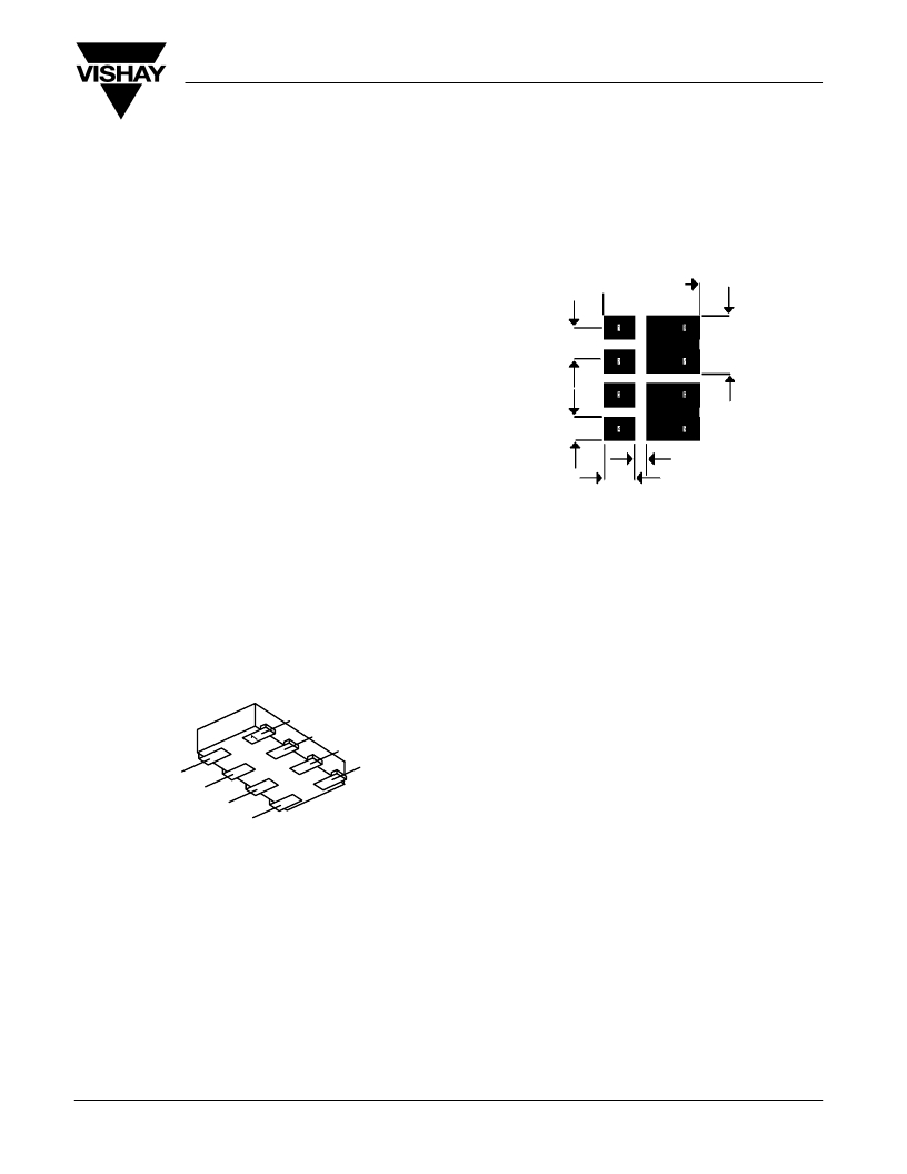
�25� mil�
�18� mil�
�80� mil�
�10� mil�
�43� mil�
�PIN-OUT�
�FIGURE� 2.�
�26� mil�
�Footprint� With� Copper� Spreading�
�Figure� 1� shows� the� pin-out� description� and� Pin� 1� identification�
�for� the� dual-channel� 1206-8� ChipFET� device.� The� pin-out� is�
�similar� to� the� TSOP-6� configuration,� with� two� additional� drain�
�pins� to� enhance� power� dissipation� and� thus� thermal�
�performance.� The� legs� of� the� device� are� very� short,� again�
�helping� to� reduce� the� thermal� path� to� the� external� heatsink/pcb�
�and� allowing� a� larger� die� to� be� fitted� in� the� device� if� necessary.�
�Dual� 1206-8� ChipFET�
�S� 1�
�G� 1�
�S� 2�
�G� 2�
�The� pad� pattern� with� copper� spreading� shown� in� Figure� 2�
�improves� the� thermal� area� of� the� drain� connections� (pins� 5� and�
�6,� pins� 7� and� 8)� while� remaining� within� the� confines� of� the� basic�
�footprint.� The� drain� copper� area� is� 0.0019� sq.� in.� or�
�1.22� sq.� mm.� This� will� assist� the� power� dissipation� path� away�
�from� the� device� (through� the� copper� leadframe)� and� into� the�
�board� and� exterior� chassis� (if� applicable)� for� the� dual� device.�
�The� addition� of� a� further� copper� area� and/or� the� addition� of� vias�
�to� other� board� layers� will� enhance� the� performance� still� further.�
�An� example� of� this� method� is� implemented� on� the� Vishay�
�Siliconix� Evaluation� Board� described� in� the� next� section�
�(Figure� 3).�
�D� 1�
�D� 1�
�D� 2�
�THE� VISHAY� SILICONIX� EVALUATION�
�BOARD� FOR� THE� DUAL� 1206-8�
�D� 2�
�FIGURE� 1.�
�For� package� dimensions� see� the� 1206-8� ChipFET� package�
�outline� drawing� (� http://www.vishay.com/doc?71151� ).�
�BASIC� PAD� PATTERNS�
�The� basic� pad� layout� with� dimensions� is� shown� in� Application�
�Note� 826,� Recommended� Minimum� Pad� Patterns� With� Outline�
�Drawing� Access� for� Vishay� Siliconix� MOSFET� s,�
�(� http://www.vishay.com/doc?72286� ).� This� is� sufficient� for� low�
�power� dissipation� MOSFET� applications,� but� power�
�semiconductor� performance� requires� a� greater� copper� pad�
�area,� particularly� for� the� drain� leads.�
�Document� Number:� 71127�
�12-Dec-03�
�The� dual� ChipFET� 1206-08� evaluation� board� measures� 0.6� in�
�by� 0.5� in.� Its� copper� pad� pattern� consists� of� an� increased� pad�
�area� around� each� of� the� two� drain� leads� on� the� top-side—�
�approximately� 0.0246� sq.� in.� or� 15.87� sq.� mm—and� vias�
�added� through� to� the� underside� of� the� board,� again� with� a�
�maximized� copper� pad� area� of� approximately� the� board-size�
�dimensions,� split� into� two� for� each� of� the� drains.� The� outer�
�package� outline� is� for� the� 8-pin� DIP,� which� will� allow� test�
�sockets� to� be� used� to� assist� in� testing.�
�The� thermal� performance� of� the� 1206-8� on� this� board� has� been�
�measured� with� the� results� following� on� the� next� page.� The�
�testing� included� comparison� with� the� minimum� recommended�
�footprint� on� the� evaluation� board-size� pcb� and� the� industry�
�standard� one-inch� square� FR4� pcb� with� copper� on� both� sides�
�of� the� board.�
�www.vishay.com�
�1�
�相关PDF资料 |
PDF描述 |
|---|---|
| SI5935DC-T1-GE3 | MOSFET DUAL P-CH 20V 1206-8 |
| SI5943DU-T1-GE3 | MOSFET DUAL P-CH 12V 6A 8PWRPAK |
| SI5975DC-T1-GE3 | MOSFET 2P-CH 12V 3.1A CHIPFET |
| SI5980DU-T1-GE3 | MOSFET N-CH 100V PPAK CHIPFET |
| SI6404DQ-T1-GE3 | MOSFET N-CH 30V 8.6A 8TSSOP |
相关代理商/技术参数 |
参数描述 |
|---|---|
| SI5935CDC | 制造商:VISHAY 制造商全称:Vishay Siliconix 功能描述:Dual P-Channel 20-V (D-S) MOSFET |
| SI5935CDC-T1-E3 | 功能描述:MOSFET 20V 4.0A 3.1W 100mohm @ 4.5V RoHS:否 制造商:STMicroelectronics 晶体管极性:N-Channel 汲极/源极击穿电压:650 V 闸/源击穿电压:25 V 漏极连续电流:130 A 电阻汲极/源极 RDS(导通):0.014 Ohms 配置:Single 最大工作温度: 安装风格:Through Hole 封装 / 箱体:Max247 封装:Tube |
| SI5935CDC-T1-GE3 | 功能描述:MOSFET 20V 4A 3.1W RoHS:否 制造商:STMicroelectronics 晶体管极性:N-Channel 汲极/源极击穿电压:650 V 闸/源击穿电压:25 V 漏极连续电流:130 A 电阻汲极/源极 RDS(导通):0.014 Ohms 配置:Single 最大工作温度: 安装风格:Through Hole 封装 / 箱体:Max247 封装:Tube |
| SI5935DC | 制造商:VISHAY 制造商全称:Vishay Siliconix 功能描述:Dual P-Channel 1.8-V (G-S) MOSFET |
| SI5935DC-T1 | 制造商:VISHAY 制造商全称:Vishay Siliconix 功能描述:Dual P-Channel 1.8-V (G-S) MOSFET |
发布紧急采购,3分钟左右您将得到回复。