- 您现在的位置:买卖IC网 > Datasheet目录512 > SI7148DP-T1-GE3 (Vishay Siliconix)MOSFET N-CH D-S 75V PPAK 8SOIC Datasheet资料下载
参数资料
| 型号: | SI7148DP-T1-GE3 |
| 厂商: | Vishay Siliconix |
| 文件页数: | 2/10页 |
| 文件大小: | 0K |
| 描述: | MOSFET N-CH D-S 75V PPAK 8SOIC |
| 标准包装: | 3,000 |
| 系列: | TrenchFET® |
| FET 型: | MOSFET N 通道,金属氧化物 |
| FET 特点: | 逻辑电平门 |
| 漏极至源极电压(Vdss): | 75V |
| 电流 - 连续漏极(Id) @ 25° C: | 28A |
| 开态Rds(最大)@ Id, Vgs @ 25° C: | 11 毫欧 @ 15A,10V |
| Id 时的 Vgs(th)(最大): | 2.5V @ 250µA |
| 闸电荷(Qg) @ Vgs: | 100nC @ 10V |
| 输入电容 (Ciss) @ Vds: | 2900pF @ 35V |
| 功率 - 最大: | 96W |
| 安装类型: | 表面贴装 |
| 封装/外壳: | PowerPAK? SO-8 |
| 供应商设备封装: | PowerPAK? SO-8 |
| 包装: | 带卷 (TR) |
�� �
�
�Si7148DP�
�Vishay� Siliconix�
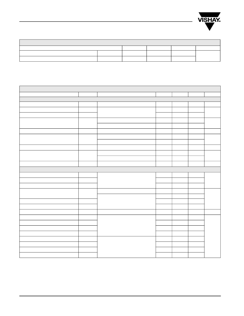
�THERMAL� RESISTANCE� RATINGS�
�Parameter�
�Symbol�
�Typical�
�Maximum�
�Unit�
�Maximum� Junction-to-Ambient�
�a,� b�
�Maximum� Junction-to-Case� (Drain)�
�t� ≤� 10� s�
�Steady� State�
�R� thJA�
�R� thJC�
�18�
�1.0�
�23�
�1.3�
�°C/W�
�Notes:�
�a.� Surface� Mounted� on� 1"� x� 1"� FR4� board.�
�b.� Maximum� under� Steady� State� conditions� is� 65� °C/W.�
�SPECIFICATIONS� T� J� =� 25� °C,� unless� otherwise� noted�
�Parameter�
�Symbol�
�Test� Conditions�
�Min.�
�Typ.�
�Max.�
�Unit�
�Static�
�Drain-Source� Breakdown� Voltage�
�V� DS� Temperature� Coefficient�
�V� GS(th)� Temperature� Coefficient�
�V� DS�
�Δ� V� DS� /T� J�
�Δ� V� GS(th)� /T� J�
�V� GS� =� 0� V,� I� D� =� 250� μA�
�I� D� =� 250� μA�
�75�
�75�
�-6�
�V�
�mV/°C�
�Gate-Source� Threshold� Voltage�
�V� GS(th)�
�V� DS� =� V� GS� ,� I� D� =� 250� μA�
�V� DS� =� V� GS� ,� I� D� =� 5� mA�
�1.5�
�2.0�
�2.3�
�2.5�
�V�
�Gate-Source� Leakage�
�Zero� Gate� Voltage� Drain� Current�
�On-State� Drain� Current� a�
�I� GSS�
�I� DSS�
�I� D(on)�
�V� DS� =� 0� V,� V� GS� =� ±� 20� V�
�V� DS� =� 75� V,� V� GS� =� 0� V�
�V� DS� =� 75� V,� V� GS� =� 0� V,� T� J� =� 55� °C�
�V� DS� ≥� 5� V,� V� GS� =� 10� V�
�30�
�±� 100�
�1�
�10�
�nA�
�μA�
�A�
�Drain-Source� On-State� Resistance� a�
�Forward� Transconductance� a�
�R� DS(on)�
�g� fs�
�V� GS� =� 10� V,� I� D� =� 15� A�
�V� GS� =� 4.5� V,� I� D� =� 13.5� A�
�V� DS� =� 15� V,� I� D� =� 15� A�
�0.0091�
�0.012�
�60�
�0.011�
�0.0145�
�Ω�
�S�
�Dynamic�
�b�
�Input� Capacitance�
�C� iss�
�2900�
�Output� Capacitance�
�Reverse� Transfer� Capacitance�
�C� oss�
�C� rss�
�V� DS� =� 35� V,� V� GS� =� 0� V,� f� =� 1� MHz�
�370�
�196�
�pF�
�Total� Gate� Charge�
�Gate-Source� Charge�
�Q� g�
�Q� gs�
�V� DS� =� 38� V,� V� GS� =� 10� V,� I� D� =� 15� A�
�V� DS� =� 38� V,� V� GS� =� 4.5� V,� I� D� =� 15� A�
�68�
�33�
�9.5�
�100�
�50�
�nC�
�Gate-Drain� Charge�
�Q� gd�
�16.8�
�Gate� Resistance�
�R� g�
�f� =� 1� MHz�
�0.5�
�1.1�
�1.7�
�Ω�
�Turn-On� Delay� Time�
�t� d(on)�
�33�
�50�
�Rise� Time�
�Turn-Off� Delay� Time�
�t� r�
�t� d(off)�
�V� DD� =� 38� V,� R� L� =� 3.8� Ω�
�I� D� ?� 10� A,� V� GEN� =� 4.5� V,� R� g� =� 1� Ω�
�255�
�35�
�390�
�55�
�Fall� Time�
�Turn-On� Delay� Time�
�t� f�
�t� d(on)�
�100�
�17�
�150�
�26�
�ns�
�Rise� Time�
�Turn-Off� Delay� Time�
�Fall� Time�
�t� r�
�t� d(off)�
�t� f�
�V� DD� =� 38� V,� R� L� =� 3.8� Ω�
�I� D� ?� 10� A,� V� GEN� =� 10� V,� R� g� =� 1� Ω�
�46�
�39�
�18�
�70�
�60�
�30�
�www.vishay.com�
�2�
�Document� Number:� 73314�
�S09-0273-Rev.� B,� 16-Feb-09�
�相关PDF资料 |
PDF描述 |
|---|---|
| SI7170DP-T1-GE3 | MOSFET N-CH 30V 40A PPAK 8SOIC |
| SI7172DP-T1-GE3 | MOSFET N-CH 200V 25A PPAK 8SOIC |
| SI7196DP-T1-E3 | MOSFET N-CH D-S 30V PPAK 8SOIC |
| SI7216DN-T1-GE3 | MOSFET DL N-CH 40V PPAK 1212-8 |
| SI7222DN-T1-GE3 | MOSFET N-CH D-S 40V 1212-8 PPAK |
相关代理商/技术参数 |
参数描述 |
|---|---|
| SI7149ADP-T1-GE3 | 制造商:Vishay Siliconix 功能描述:MOSFET P-CH 30V PPAK SO-8 制造商:Vishay Intertechnologies 功能描述:MOSFET -30V 5.2mOhm@10V -50A P-Ch G-III |
| SI7149DP-T1-E3 | 制造商:Vishay Semiconductors 功能描述: |
| SI7149DP-T1-GE3 | 功能描述:MOSFET 30V 50A 69W 5.2mohm @ 10V RoHS:否 制造商:STMicroelectronics 晶体管极性:N-Channel 汲极/源极击穿电压:650 V 闸/源击穿电压:25 V 漏极连续电流:130 A 电阻汲极/源极 RDS(导通):0.014 Ohms 配置:Single 最大工作温度: 安装风格:Through Hole 封装 / 箱体:Max247 封装:Tube |
| SI7156DP-T1-E3 | 功能描述:MOSFET 40V 50A 83W 3.5mohm @ 10V RoHS:否 制造商:STMicroelectronics 晶体管极性:N-Channel 汲极/源极击穿电压:650 V 闸/源击穿电压:25 V 漏极连续电流:130 A 电阻汲极/源极 RDS(导通):0.014 Ohms 配置:Single 最大工作温度: 安装风格:Through Hole 封装 / 箱体:Max247 封装:Tube |
| SI7156DP-T1-GE3 | 功能描述:MOSFET 40V 50A 83W 3.5mohm @ 10V RoHS:否 制造商:STMicroelectronics 晶体管极性:N-Channel 汲极/源极击穿电压:650 V 闸/源击穿电压:25 V 漏极连续电流:130 A 电阻汲极/源极 RDS(导通):0.014 Ohms 配置:Single 最大工作温度: 安装风格:Through Hole 封装 / 箱体:Max247 封装:Tube |
发布紧急采购,3分钟左右您将得到回复。