- 您现在的位置:买卖IC网 > PDF目录98081 > SL23EP08SC-2HT 23EP SERIES, PLL BASED CLOCK DRIVER, 4 TRUE OUTPUT(S), 0 INVERTED OUTPUT(S), PDSO16 PDF资料下载
参数资料
| 型号: | SL23EP08SC-2HT |
| 元件分类: | 时钟及定时 |
| 英文描述: | 23EP SERIES, PLL BASED CLOCK DRIVER, 4 TRUE OUTPUT(S), 0 INVERTED OUTPUT(S), PDSO16 |
| 封装: | 0.150 INCH, ROHS COMPLIANT,SOIC-16 |
| 文件页数: | 7/18页 |
| 文件大小: | 405K |
| 代理商: | SL23EP08SC-2HT |
Rev 2.0, May 28, 2008
Page 15 of 18
SL23EP08
(-2, -2H and -3 Versions)
Fout=166MHz and CL=15pF
-
400
ps
PLL Lock Time
tLOCK
From 0.95VDD and valid CLKIN
-
1.0
ms
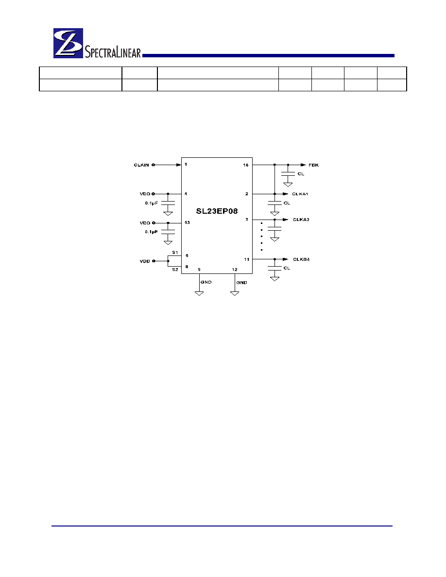
External Components & Design Considerations
Typical Application Schematic
Comments and Recommendations
Decoupling Capacitor:
A minimum decoupling capacitor of 0.1μF must be used between VDD and VSS pins.
Additional capacitors may be necessary depending on the application. Place the capacitor on the component side of
the PCB as close to the VDD pin as possible. The PCB trace to the VDD pin and to the GND via should be kept as
short as possible. Do not use vias between the decoupling capacitor and the VDD pin.
Series Termination Resistor:
A series termination resistor is recommended if the distance between the output
clocks and the load is over 1 inch. The nominal impedance of the clock outputs is given on the Operating
Conditions Tables. Place the series termination resistors as close to the clock outputs as possible.
Zero Delay and Skew Control:
All outputs and CLKIN pins should be loaded with the same load to achieve “Zero
Delay” between the CLKIN and the outputs. The CLKOUT pin is connected to CLKIN internally on-chip for feedback
to PLL. For applications requiring zero input/output delay, the load at the all output pins including the CLKOUT pin
must be the same. If any delay adjustment is required, the capacitance at the CLKOUT pin could be increased or
decreased to increase or decrease the delay between Bank A and B clocks and CLKIN. For minimum pin-to-pin
skew, the external load at all the Bank A and B clocks must be the same.
相关PDF资料 |
PDF描述 |
|---|---|
| SL23EP08ZC-1T | PLL BASED CLOCK DRIVER, PDSO16 |
| SL23EP08SI-2 | 23EP SERIES, PLL BASED CLOCK DRIVER, 4 TRUE OUTPUT(S), 0 INVERTED OUTPUT(S), PDSO16 |
| SL23EP08SC-4 | 23EP SERIES, PLL BASED CLOCK DRIVER, 4 TRUE OUTPUT(S), 0 INVERTED OUTPUT(S), PDSO16 |
| SL23EP08SC-2T | 23EP SERIES, PLL BASED CLOCK DRIVER, 4 TRUE OUTPUT(S), 0 INVERTED OUTPUT(S), PDSO16 |
| SL23EP08SI-1H | 23EP SERIES, PLL BASED CLOCK DRIVER, 4 TRUE OUTPUT(S), 0 INVERTED OUTPUT(S), PDSO16 |
相关代理商/技术参数 |
参数描述 |
|---|---|
| SL23EP08SC-2T | 功能描述:时钟缓冲器 10-220MHz 8 Outputs ZDB 3.3-2.5V RoHS:否 制造商:Texas Instruments 输出端数量:5 最大输入频率:40 MHz 传播延迟(最大值): 电源电压-最大:3.45 V 电源电压-最小:2.375 V 最大功率耗散: 最大工作温度:+ 85 C 最小工作温度:- 40 C 封装 / 箱体:LLP-24 封装:Reel |
| SL23EP08SC-3 | 功能描述:时钟缓冲器 10-220MHz 8 Outputs ZDB 3.3-2.5V RoHS:否 制造商:Texas Instruments 输出端数量:5 最大输入频率:40 MHz 传播延迟(最大值): 电源电压-最大:3.45 V 电源电压-最小:2.375 V 最大功率耗散: 最大工作温度:+ 85 C 最小工作温度:- 40 C 封装 / 箱体:LLP-24 封装:Reel |
| SL23EP08SC-3T | 功能描述:时钟缓冲器 10-220MHz 8 Outputs ZDB 3.3-2.5V RoHS:否 制造商:Texas Instruments 输出端数量:5 最大输入频率:40 MHz 传播延迟(最大值): 电源电压-最大:3.45 V 电源电压-最小:2.375 V 最大功率耗散: 最大工作温度:+ 85 C 最小工作温度:- 40 C 封装 / 箱体:LLP-24 封装:Reel |
| SL23EP08SC-4 | 功能描述:时钟缓冲器 10-220MHz 8 Outputs ZDB 3.3-2.5V RoHS:否 制造商:Texas Instruments 输出端数量:5 最大输入频率:40 MHz 传播延迟(最大值): 电源电压-最大:3.45 V 电源电压-最小:2.375 V 最大功率耗散: 最大工作温度:+ 85 C 最小工作温度:- 40 C 封装 / 箱体:LLP-24 封装:Reel |
| SL23EP08SC-4H | 功能描述:时钟缓冲器 10-220MH 8 Outputs ZDB 3.3-2.5V RoHS:否 制造商:Texas Instruments 输出端数量:5 最大输入频率:40 MHz 传播延迟(最大值): 电源电压-最大:3.45 V 电源电压-最小:2.375 V 最大功率耗散: 最大工作温度:+ 85 C 最小工作温度:- 40 C 封装 / 箱体:LLP-24 封装:Reel |
发布紧急采购,3分钟左右您将得到回复。