- 您现在的位置:买卖IC网 > PDF目录98083 > SM320C6701GLPW16 (TEXAS INSTRUMENTS INC) 32-BIT, 167 MHz, OTHER DSP, CBGA429 PDF资料下载
参数资料
| 型号: | SM320C6701GLPW16 |
| 厂商: | TEXAS INSTRUMENTS INC |
| 元件分类: | 数字信号处理 |
| 英文描述: | 32-BIT, 167 MHz, OTHER DSP, CBGA429 |
| 封装: | CERAMIC, BGA-429 |
| 文件页数: | 61/62页 |
| 文件大小: | 873K |
| 代理商: | SM320C6701GLPW16 |
第1页第2页第3页第4页第5页第6页第7页第8页第9页第10页第11页第12页第13页第14页第15页第16页第17页第18页第19页第20页第21页第22页第23页第24页第25页第26页第27页第28页第29页第30页第31页第32页第33页第34页第35页第36页第37页第38页第39页第40页第41页第42页第43页第44页第45页第46页第47页第48页第49页第50页第51页第52页第53页第54页第55页第56页第57页第58页第59页第60页当前第61页第62页
SMJ320C6701
FLOATINGPOINT DIGITAL SIGNAL PROCESSOR
SGUS030A – APRIL 2000 – REVISED APRIL 2001
8
POST OFFICE BOX 655303
DALLAS, TEXAS 75265
POST OFFICE BOX 1443
HOUSTON, TEXAS 77251–1443
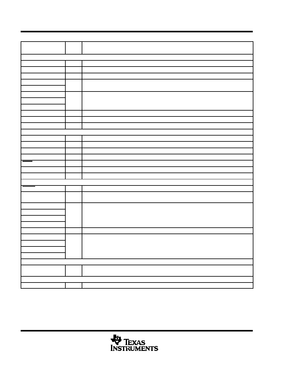
Signal Descriptions
SIGNAL
TYPE
DESCRIPTION
NAME
NO.
TYPE
DESCRIPTION
CLOCK/PLL
CLKIN
A14
I
Clock Input
CLKOUT1
Y6
O
Clock output at full device speed
CLKOUT2
V9
O
Clock output at half of device speed
CLKMODE1
B17
I
Clock mode select
CLKMODE0
C17
I
Selects whether the output clock frequency = input clock freq x4 or x1
PLLFREQ3
C13
PLL frequency range (3, 2, and 1)
PLLFREQ2
G11
I
The target range for CLKOUT1 frequency is determined by the 3-bit value of the PLLFREQ pins.
PLLFREQ1
F11
I
PLLV
D12
A§
PLL analog VCC connection for the low-pass filter
PLLG
G10
A§
PLL analog GND connection for the low-pass filter
PLLF
C12
A§
PLL low-pass filter connection to external components and a bypass capacitor
JTAG EMULATION
TMS
K19
I
JTAG test port mode select (features an internal pull-up)
TDO
R12
O/Z
JTAG test port data out
TDI
R13
I
JTAG test port data in (features an internal pull-up)
TCK
M20
I
JTAG test port clock
TRST
N18
I
JTAG test port reset (features an internal pull-down)
EMU1
R20
I/O/Z
Emulation pin 1, pull-up with a dedicated 20-k
resistor
EMU0
T18
I/O/Z
Emulation pin 0, pull-up with a dedicated 20-k
resistor
RESET AND INTERRUPTS
RESET
J20
I
Device reset
NMI
K21
I
Nonmaskable interrupt
Edge-driven (rising edge)
EXT_INT7
R16
EXT_INT6
P20
I
External interrupts
EXT_INT5
R15
I
External interru ts
Edge-driven (rising edge)
EXT_INT4
R18
gg
g
IACK
R11
O
Interrupt acknowledge for all active interrupts serviced by the CPU
INUM3
T19
INUM2
T20
O
Active interrupt identification number
Valid during IACK for all active interrupts (not just external)
INUM1
T14
O
Valid during IACK for all active interrupts (not just external)
Encoding order follows the interrupt service fetch packet ordering
INUM0
T16
Encoding order follows the interru t service fetch acket ordering
LITTLE ENDIAN/BIG ENDIAN
LENDIAN
G20
I
If high, selects little-endian byte/half-word addressing order within a word
If low, selects big-endian addressing
POWER DOWN STATUS
PD
D19
O
Power-down mode 2 or 3 (active if high)
I = Input, O = Output, Z = High Impedance, S = Supply Voltage, GND = Ground
PLLV and PLLG signals are not part of external voltage supply or ground. See the CLOCK/PLL documentation for information on how to connect
those pins.
§ A = Analog Signal (PLL Filter)
相关PDF资料 |
PDF描述 |
|---|---|
| SM320C6701GLPS14 | 32-BIT, 140 MHz, OTHER DSP, CBGA429 |
| SM320C80GFM40 | 64-BIT, 80 MHz, OTHER DSP, CPGA305 |
| SM320F2812HFGM | 16-BIT, 150 MHz, OTHER DSP, CQFP172 |
| SM320MCM41DHFHM40 | 32-BIT, 40 MHz, OTHER DSP, CQFP352 |
| SM320MCM42CHFNM40 | 32-BIT, 40 MHz, OTHER DSP, CQFP408 |
相关代理商/技术参数 |
参数描述 |
|---|---|
| SM320C6701S14 | 制造商:TI 制造商全称:Texas Instruments 功能描述:FLOATING-POINT DIGITAL SIGNAL PROCESSOR |
| SM320C6701S16 | 制造商:TI 制造商全称:Texas Instruments 功能描述:FLOATING-POINT DIGITAL SIGNAL PROCESSOR |
| SM320C6701W14 | 制造商:TI 制造商全称:Texas Instruments 功能描述:FLOATING-POINT DIGITAL SIGNAL PROCESSOR |
| SM320C6701W16 | 制造商:TI 制造商全称:Texas Instruments 功能描述:FLOATING-POINT DIGITAL SIGNAL PROCESSOR |
| SM320C6701ZMBW14 | 功能描述:数字信号处理器和控制器 - DSP, DSC Floating Point Dig Signal Proc Military RoHS:否 制造商:Microchip Technology 核心:dsPIC 数据总线宽度:16 bit 程序存储器大小:16 KB 数据 RAM 大小:2 KB 最大时钟频率:40 MHz 可编程输入/输出端数量:35 定时器数量:3 设备每秒兆指令数:50 MIPs 工作电源电压:3.3 V 最大工作温度:+ 85 C 封装 / 箱体:TQFP-44 安装风格:SMD/SMT |
发布紧急采购,3分钟左右您将得到回复。