- 您现在的位置:买卖IC网 > PDF目录97020 > SM561BZ (CYPRESS SEMICONDUCTOR CORP) 166 MHz, PROC SPECIFIC CLOCK GENERATOR, PDSO8 PDF资料下载
参数资料
| 型号: | SM561BZ |
| 厂商: | CYPRESS SEMICONDUCTOR CORP |
| 元件分类: | 时钟产生/分配 |
| 英文描述: | 166 MHz, PROC SPECIFIC CLOCK GENERATOR, PDSO8 |
| 封装: | SOIC-8 |
| 文件页数: | 7/10页 |
| 文件大小: | 75K |
| 代理商: | SM561BZ |
Spread Spectrum Clock Generator
CYPRESS SEMICONDUCTOR CORPORATION 525 Los Coches St.
Document#: 38-07021 Rev. **
05/04/2001
MILPITAS, CA 95035 TEL: 408-263-6300, FAX 408-263-6571
Page 6 of 10
http://www.cypress.com
APPROVED PRODUCT
SM561
SSCG Theory of Operation
The SM561 is a Phase Lock Loop (PLL) type clock generator using a proprietary Cypress design.
By precisely
controlling the bandwidth of the output clock, the SM561 becomes a Low EMI clock generator. The theory and
detailed operation of the SM561 will be discussed in the following sections.
EMI
All digital clocks generate unwanted energy in their harmonics. Conventional digital clocks are square waves with
a duty cycle that is very close to 50 %. Because of this 50/50-duty cycle, digital clocks generate most of their
harmonic energy in the odd harmonics, i.e.; 3
rd, 5th, 7th etc. It is possible to reduce the amount of energy
contained in the fundamental and odd harmonics by increasing the bandwidth of the fundamental clock frequency.
Conventional digital clocks have a very high Q factor, which means that all of the energy at that frequency is
concentrated in a very narrow bandwidth, consequently, higher energy peaks.
Regulatory agencies test
electronic equipment by the amount of peak energy radiated from the equipment. By reducing the peak energy at
the fundamental and harmonic frequencies, the equipment under test is able to satisfy agency requirements for
Electro-Magnetic Interference (EMI). Conventional methods of reducing EMI have been to use shielding, filtering,
multi-layer PCB’s etc. The SM561 uses the approach of reducing the peak energy in the clock by increasing the
clock bandwidth, and lowering the Q.
SSCG
SSCG uses a patented technology of modulating the clock over a very narrow bandwidth and controlled rate of
change, both peak and cycle to cycle. The SM561 takes a narrow band digital reference clock in the range of 27 -
108 MHz and produces a clock that sweeps between a controlled start and stop frequency and precise rate of
change. To understand what happens to a clock when SSCG is applied, consider a 65 MHz clock with a 50 %
duty cycle. From a 65 MHz clock we know the following;
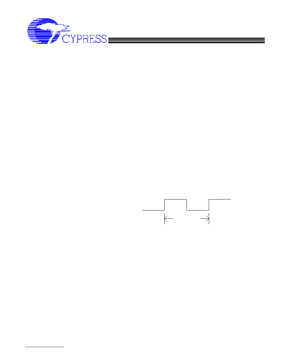
Clock Frequency = fc = 65 MHz.
Clock Period = Tc = 1/65 MHz = 15.4 ns.
If this clock is applied to the Xin/CLK pin of the SM561, the output clock at pin 4 (SSCLK) will be sweeping back
and forth between two frequencies. These two frequencies, F1 and F2, are used to calculate to total amount of
spread or bandwidth applied to the reference clock at pin 1. As the clock is making the transition from f1 to f2, the
amount of time and sweep waveform play a very important role in the amount of EMI reduction realized from an
SSCG clock.
The modulation domain analyzer is used to visualize the sweep waveform and sweep period. Figure 3 shows the
modulation profile of a 65 MHz SSCG clock. Notice that the actual sweep waveform is not a simple sine or
sawtooth waveform. Figure 4 is a scan of the same SSCG clock using a spectrum analyzer. In this scan you can
see a 6.48 dB reduction in the peak RF energy when using the SSCG clock.
Tc = 15.4 ns
50 %
相关PDF资料 |
PDF描述 |
|---|---|
| SM6010 | 16-BIT, MICROCONTROLLER, PQFP100 |
| SM802111UMG | 111 SERIES, PLL BASED CLOCK DRIVER, 2 TRUE OUTPUT(S), 0 INVERTED OUTPUT(S), QCC24 |
| SM8206 | 8-BIT, MROM, MICROCONTROLLER, PQFP80 |
| SM840002KA | 156.25 MHz, OTHER CLOCK GENERATOR, PDSO16 |
| SM840021KATR | 125 MHz, OTHER CLOCK GENERATOR, PDSO8 |
相关代理商/技术参数 |
参数描述 |
|---|---|
| SM561C107KAN360 | 制造商:AVX Corporation 功能描述:- Bulk |
| SM561K | 制造商:CDE 制造商全称:Cornell Dubilier Electronics 功能描述:Ceramic Capacitors |
| SM562-1 | 功能描述:变压器音频和信号 Line Transformer RoHS:否 制造商:Skyworks Solutions, Inc. 频率范围:810 MHz to 960 MHz 初级线圈阻抗: 次级线圈阻抗: 绝缘电压:23 dB 工作温度范围:- 40 C to + 85 C 端接类型:SMD/SMT 尺寸:6 mm L x 4.9 mm W x 1.6 mm H 产品:Splitters and Combiners |
| SM562-1EL | 制造商:BOURNS 制造商全称:Bourns Electronic Solutions 功能描述:ADSL Line Transformers |
| SM562-1L | 功能描述:变压器音频和信号 Magnetics RoHS:否 制造商:Skyworks Solutions, Inc. 频率范围:810 MHz to 960 MHz 初级线圈阻抗: 次级线圈阻抗: 绝缘电压:23 dB 工作温度范围:- 40 C to + 85 C 端接类型:SMD/SMT 尺寸:6 mm L x 4.9 mm W x 1.6 mm H 产品:Splitters and Combiners |
发布紧急采购,3分钟左右您将得到回复。