参数资料
| 型号: | SMP18FS-REEL |
| 厂商: | Analog Devices Inc |
| 文件页数: | 6/8页 |
| 文件大小: | 0K |
| 描述: | IC AMP SAMPLE HOLD OCTAL 16SOIC |
| 标准包装: | 2,500 |
| 放大器类型: | 采样和保持 |
| 电路数: | 8 |
| 转换速率: | 7 V/µs |
| 电流 - 输入偏压: | 500nA |
| 电压 - 输入偏移: | 2500µV |
| 电流 - 电源: | 6mA |
| 电流 - 输出 / 通道: | 1.2mA |
| 电压 - 电源,单路/双路(±): | 5 V ~ 12 V,±2.5 V ~ 6 V |
| 工作温度: | -40°C ~ 85°C |
| 安装类型: | 表面贴装 |
| 封装/外壳: | 16-SOIC(0.154",3.90mm 宽) |
| 供应商设备封装: | 16-SOIC |
| 包装: | 带卷 (TR) |
SMP18
REV. C
–6–
14
13
12
11
16
15
10
9
8
1
2
3
4
7
6
5
SMP18
R3
2k
R4
1k
R1
10
D1
C1
10F
C2
1F
+
VCC
+15V
R2
10k
R2
10k
R2
10k
R2
10k
R2
10k
R2
10k
R2
10k
R2
10k
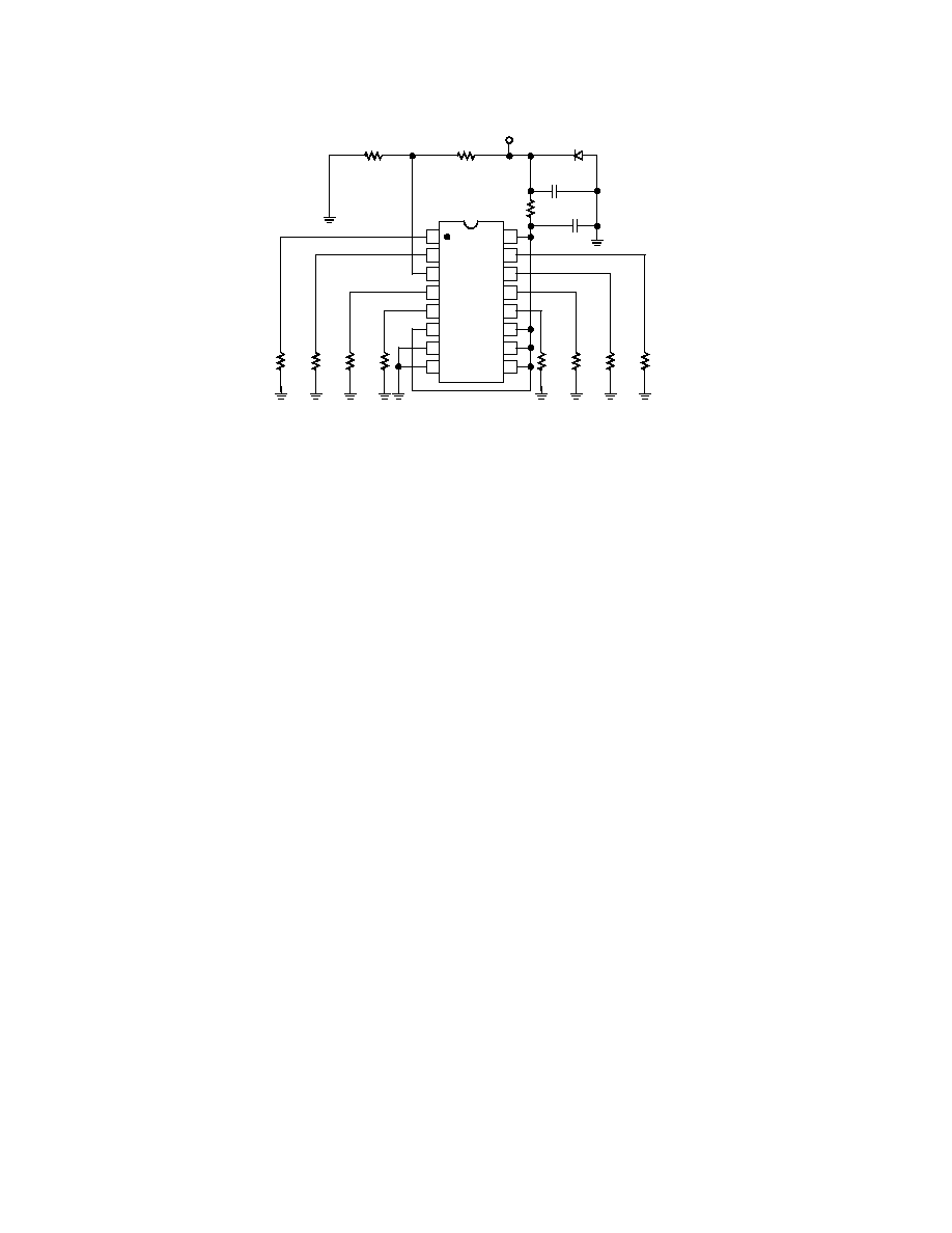
Burn-in Circuit
APPLICATIONS INFORMATION
The SMP18, a multiplexed octal S/H, minimizes board space
in systems requiring cycled calibration or an array of control
voltages. When used in conjunction with a low cost 16-bit D/A,
the SMP18 can easily be integrated into microprocessor based
systems. Since the SMP18 features break-before-make switching
and an internal decoder, no external logic is required. The
SMP18 has an internally regulated TTL supply so that
TTL/CMOS compatibility is maintained over the full supply
range. See Figure 1 for channel decode address information.
POWER SUPPLIES
The SMP18 is capable of operating with either single or dual
supplies over a voltage range of 7 to 15 volts. Based on the sup-
ply voltages chosen, VDD and VSS establish the output voltage
range, which is:
(VSS + 0.06 V ) ≤ VOUT ≤ (VDD – 2 V )
Note that several specifications, including acquisition time, off-
set and output voltage compliance, will degrade for supply volt-
ages of less than 7 V.
If split supplies are used, the negative supply should be bypassed
with a 0.1
F capacitor in parallel with a 10 F to ground. The
internal hold capacitors are connected to this supply pin, and
any noise will appear at the outputs.
In single supply applications, it is extremely important that the
VSS (negative supply) pin is connected to a clean ground. The
hold capacitors are internally tied to the VSS (negative) rail. Any
ground noise or disturbance will directly couple to the output of
the sample-and-hold degrading the signal-to-noise performance.
The analog and digital ground traces on the circuit board should
be physically separated to reduce digital switching noise from
entering the analog circuitry.
POWER SUPPLY SEQUENCING
VDD should be applied to the SMP18 before the logic input sig-
nals. The SMP18 has been designed to be immune to latchup,
but standard precautions should still be taken.
OUTPUT BUFFERS (Pins 1, 2, 4, 5, 12, 13, 14, 15)
The buffer offset specification is 10 mV; this is less than 1/2
LSB of an 8-bit DAC with 10 V full scale. The hold step (mag-
nitude of step caused in the output voltage when switching from
sample-to-hold mode, also referred to as the pedestal error or
sample-to-hold offset) is about 4 mV with little variation over
the full output voltage range. The droop rate of a held channel
is 2 mV/s typical and 40 mV/s maximum.
The buffers are designed to drive loads connected to ground.
The outputs can source more than 20 mA over the full voltage
range but have limited current sinking capability near VSS. In
split supply operation, symmetrical output swings can be ob-
tained by restricting the output range to 2 V from either supply.
On-chip SMP18 buffers eliminate potential stability problems
associated with external buffers; outputs are stable with capaci-
tive loads up to 500 pF. However, since the SMP18’s buffer
outputs are not short circuit protected, care should be taken to
avoid shorting any output to the supplies or ground.
SIGNAL INPUT (Pin 3)
The signal input should be driven from a low impedance voltage
source such as the output of an op amp. The op amp should
have a high slew rate and fast settling time if the SMP18’s ac-
quisition time characteristics are to be maintained. As with all
CMOS devices, all input voltages should be kept within range of
the supply rails (VSS
≤ V
IN
≤ V
DD) to avoid the possibility of
latchup. If single supply operation is desired, op amps such as
the OP183 or AD820 that have input and output voltage com-
pliances including ground, can be used to drive the inputs. Split
supplies, such as
±7.5 V, can be used with the SMP18.
相关PDF资料 |
PDF描述 |
|---|---|
| 69192-164HLF | BERGSTIK II DR STRAIGHT RET |
| AD842KNZ | IC OPAMP GP 80MHZ 100MA 14DIP |
| DF7-6P-3.96DS | CONN HEADER 6POS 3.96MM RT ANG T |
| TSM-108-01-TM-DV-P | CONN HEADER 16POS .100" DBL SMD |
| OP467GS-REEL | IC OPAMP GP 28MHZ QUAD 16SOIC |
相关代理商/技术参数 |
参数描述 |
|---|---|
| SMP18FSZ | 功能描述:IC AMP SAMPLE HOLD OCTAL 16SOIC RoHS:是 类别:集成电路 (IC) >> Linear - Amplifiers - Instrumentation 系列:- 标准包装:1 系列:- 放大器类型:通用 电路数:4 输出类型:满摆幅 转换速率:0.028 V/µs 增益带宽积:105kHz -3db带宽:- 电流 - 输入偏压:3nA 电压 - 输入偏移:100µV 电流 - 电源:3.3µA 电流 - 输出 / 通道:12mA 电压 - 电源,单路/双路(±):2.7 V ~ 12 V,±1.35 V ~ 6 V 工作温度:-40°C ~ 85°C 安装类型:表面贴装 封装/外壳:14-TSSOP(0.173",4.40mm 宽) 供应商设备封装:14-TSSOP 包装:剪切带 (CT) 其它名称:OP481GRUZ-REELCT |
| SMP18FSZ-REEL | 功能描述:IC AMP SAMPLE HOLD OCTAL 16SOIC RoHS:是 类别:集成电路 (IC) >> Linear - Amplifiers - Instrumentation 系列:- 标准包装:2,500 系列:Excalibur™ 放大器类型:J-FET 电路数:1 输出类型:- 转换速率:45 V/µs 增益带宽积:10MHz -3db带宽:- 电流 - 输入偏压:20pA 电压 - 输入偏移:490µV 电流 - 电源:1.7mA 电流 - 输出 / 通道:48mA 电压 - 电源,单路/双路(±):4.5 V ~ 38 V,±2.25 V ~ 19 V 工作温度:-40°C ~ 85°C 安装类型:表面贴装 封装/外壳:8-SOIC(0.154",3.90mm 宽) 供应商设备封装:8-SOIC 包装:带卷 (TR) |
| SMP18-M3/84A | 功能描述:ESD 抑制器 400watt 18volt 10% Unidir RoHS:否 制造商:STMicroelectronics 通道:8 Channels 击穿电压:8 V 电容:45 pF 端接类型:SMD/SMT 封装 / 箱体:uQFN-16 功率耗散 Pd: 工作温度范围:- 40 C to + 85 C |
| SMP18-M3/85A | 功能描述:ESD 抑制器 400watt 18volt 10% Unidir RoHS:否 制造商:STMicroelectronics 通道:8 Channels 击穿电压:8 V 电容:45 pF 端接类型:SMD/SMT 封装 / 箱体:uQFN-16 功率耗散 Pd: 工作温度范围:- 40 C to + 85 C |
| SMP-18V-BC | 制造商:JST Manufacturing 功能描述: 制造商:JST Manufacturing 功能描述:Conn Housing PL 18 POS Crimp ST Bag 制造商:JST Manufacturing 功能描述:Connector,Plastic Housing Lance,Multipo |
发布紧急采购,3分钟左右您将得到回复。