- 您现在的位置:买卖IC网 > PDF目录373461 > SN54LVTH18652AHV (Texas Instruments, Inc.) Octal 3-State Noninverting Buffer/Line Driver/Line Receiver; Package: 20 LEAD PDIP; No of Pins: 20; Container: Rail; Qty per Container: 18 PDF资料下载
参数资料
| 型号: | SN54LVTH18652AHV |
| 厂商: | Texas Instruments, Inc. |
| 英文描述: | Octal 3-State Noninverting Buffer/Line Driver/Line Receiver; Package: 20 LEAD PDIP; No of Pins: 20; Container: Rail; Qty per Container: 18 |
| 中文描述: | 的3.3V ABT生根粉扫描测试设备与18位收发器和寄存器 |
| 文件页数: | 26/38页 |
| 文件大小: | 606K |
| 代理商: | SN54LVTH18652AHV |
第1页第2页第3页第4页第5页第6页第7页第8页第9页第10页第11页第12页第13页第14页第15页第16页第17页第18页第19页第20页第21页第22页第23页第24页第25页当前第26页第27页第28页第29页第30页第31页第32页第33页第34页第35页第36页第37页第38页
SN54LVTH18652A, SN54LVTH182652A, SN74LVTH18652A, SN74LVTH182652A
3.3-V ABT SCAN TEST DEVICES
WITH 18-BIT TRANSCEIVERS AND REGISTERS
SCBS312C – MARCH 1994 – REVISED JUNE 1997
26
POST OFFICE BOX 655303
DALLAS, TEXAS 75265
E
E
T
1
2
3
4
5
6
7
8
9
10
11
12
13
14
15
16
17
18
19
20
21
22
23
24
25
R
S
S
C
S
U
S
C
S
U
S
S
T
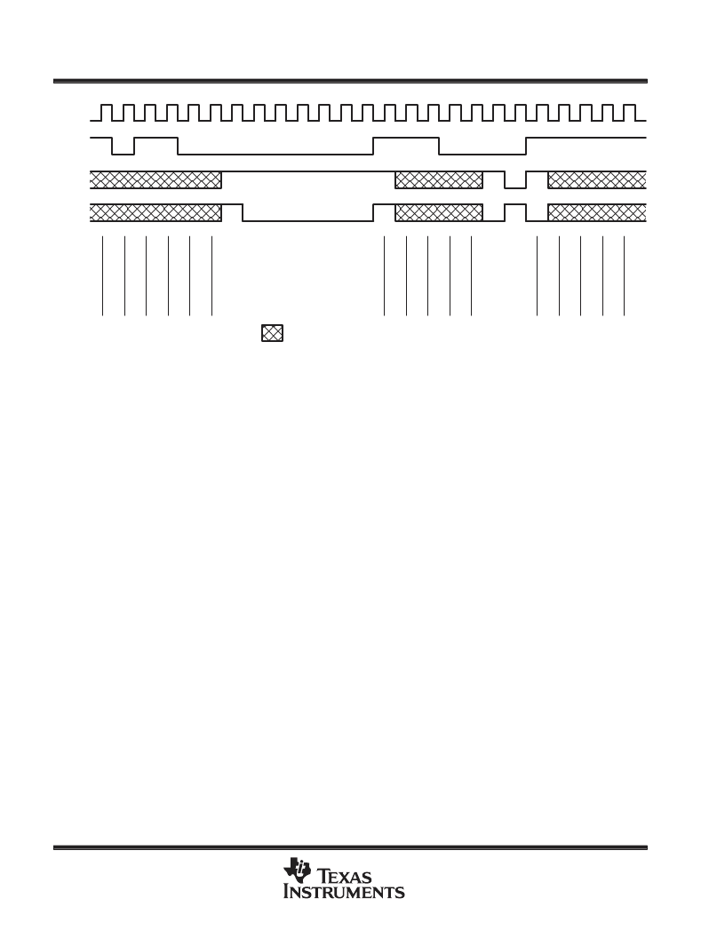
TCK
TMS
TDI
TDO
TAP
Controller
State
3-State (TDO) or Don’t Care (TDI)
Figure 14. Timing Example
absolute maximum ratings over operating free-air temperature range (unless otherwise noted)
Supply voltage range, V
CC
Input voltage range, V
I
(see Note 1)
Voltage range applied to any output in the high or power-off state, V
O
(see Note 1)
Current into any output in the low state, I
O
: SN54LVTH18652A
–0.5 V to 4.6 V
–0.5 V to 7 V
–0.5 V to 7 V
. . . . . . . . . . . . . . . . . . . . . . . . . . . . . . . . . . . . . . . . . . . . . . . . . . . . . . . . .
. . . . . . . . . . . . . . . . . . . . . . . . . . . . . . . . . . . . . . . . . . . . . . . . . .
. . . . . . . . .
96 mA
96 mA
30 mA
128 mA
128 mA
30 mA
48 mA
48 mA
30 mA
64 mA
64 mA
30 mA
–50 mA
–50 mA
67
°
C/W
. . . . . . . . . . . . . . . . . . . . . . . . . . . . . . . .
. . . . . . . . . . . . . . . .
. . . . . . . . . . . . . . . . . . . . . . .
. . . . . . . . . . . . . . . . . . . . . . . . . . . . . . .
. . . . . . . . . . . . . . .
. . . . . . . . . . . . . . . . . . . . . . .
. . . . . . . . . . . . . . . . . . . .
SN54LVTH182652A (A port or TDO)
SN54LVTH182652A (B port)
SN74LVTH18652A
. . . . . . . . . . . . . . . . . . . .
SN74LVTH182652A (A port or TDO)
SN74LVTH182652A (B port)
SN54LVTH182652A (A port or TDO)
SN54LVTH182652A (B port)
SN74LVTH18652A
SN74LVTH182652A (A port or TDO)
SN74LVTH182652A (B port)
Current into any output in the high state, I
O
(see Note 2): SN54LVTH18652A
. . . .
. . . . . . . . . . .
. . . .
. . . . . . . . . . .
Input clamp current, I
IK
(V
I
< 0)
Output clamp current, I
OK
(V
O
< 0)
Package thermal impedance,
θ
JA
(see Note 3): PM package
Storage temperature range, T
stg
Stresses beyond those listed under “absolute maximum ratings” may cause permanent damage to the device. These are stress ratings only, and
functional operation of the device at these or any other conditions beyond those indicated under “recommended operating conditions” is not
implied. Exposure to absolute-maximum-rated conditions for extended periods may affect device reliability.
NOTES:
1. The input and output negative-voltage ratings can be exceeded if the input and output clamp-current ratings are observed.
2. This current flows only when the output is in the high state and VO > VCC.
3. The package thermal impedance is calculated in accordance with JESD 51.
. . . . . . . . . . . . . . . . . . . . . . . . . . . . . . . . . . . . . . . . . . . . . . . . . . . . . . . . . . .
. . . . . . . . . . . . . . . . . . . . . . . . . . . . . . . . . . . . . . . . . . . . . . . . . . . . . . . .
. . . . . . . . . . . . . . . . . . . . . . . . . . . . . . . . . .
. . . . . . . . . . . . . . . . . . . . . . . . . . . . . . . . . . . . . . . . . . . . . . . . . . .
–65
°
C to 150
°
C
相关PDF资料 |
PDF描述 |
|---|---|
| SN54LVTH18512 | 3.3-V ABT Scan Test Device With 18-Bit Universal Bus Transceivers(3.3VABT扫描测试装置(18位通用总线收发器)) |
| SN54LVTH182512 | 3.3-V ABT Scan Test Device With 18-Bit Universal Bus Transceivers(3.3VABT扫描测试装置(18位通用总线收发器)) |
| SN54LVTH18514 | 3.3-V ABT Scan Test Device With 20-Bit Universal Bus Transceivers(3.3VABT扫描测试装置(20位通用总线收发器)) |
| SN54LVTH182514 | 3.3-V ABT Scan Test Device With 20-Bit Universal Bus Transceivers(3.3VABT扫描测试装置(20位通用总线收发器)) |
| SN74LVTH182514 | 3.3-V ABT Scan Test Device With 20-Bit Universal Bus Transceivers(3.3V ABT扫描测试装置(20位通用总线收发器)) |
相关代理商/技术参数 |
参数描述 |
|---|---|
| SN54S00J | 制造商:Texas Instruments 功能描述:NAND Gate 4-Element 2-IN Bipolar 14-Pin CDIP Tube 制造商:Rochester Electronics LLC 功能描述:- Bulk |
| SN54S00W | 制造商:Rochester Electronics LLC 功能描述:- Bulk |
| SN54S02J | 制造商:Texas Instruments 功能描述: |
| SN54S03J | 制造商:Rochester Electronics LLC 功能描述:- Bulk 制造商:Texas Instruments 功能描述:2-INPUT NAND GATE (OC) - Rail/Tube |
| SN54S04J | 制造商:Texas Instruments 功能描述:Inverter 6-Element Bipolar 14-Pin CDIP Tube 制造商:Rochester Electronics LLC 功能描述:- Bulk 制造商:Texas Instruments 功能描述:INVERTER 6-ELEM BIPOLAR 14CDIP - Rail/Tube 制造商:Texas Instruments 功能描述:HEX INVERTER *NIC* |
发布紧急采购,3分钟左右您将得到回复。