- 您现在的位置:买卖IC网 > PDF目录98102 > SN74ALVCH16903DLR (TEXAS INSTRUMENTS INC) ALVC/VCX/A SERIES, 12-BIT DRIVER, TRUE OUTPUT, PDSO56 PDF资料下载
参数资料
| 型号: | SN74ALVCH16903DLR |
| 厂商: | TEXAS INSTRUMENTS INC |
| 元件分类: | 总线收发器 |
| 英文描述: | ALVC/VCX/A SERIES, 12-BIT DRIVER, TRUE OUTPUT, PDSO56 |
| 封装: | 0.300 INCH, GREEN, PLASTIC, SSOP-56 |
| 文件页数: | 1/18页 |
| 文件大小: | 401K |
| 代理商: | SN74ALVCH16903DLR |
www.ti.com
FEATURES
DESCRIPTION
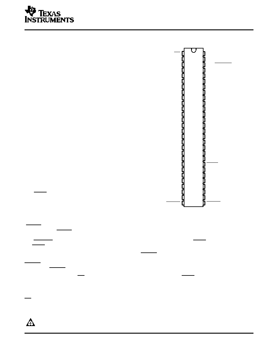
DGG, DGV, OR DL PACKAGE
(TOP VIEW)
1
2
3
4
5
6
7
8
9
10
11
12
13
14
15
16
17
18
19
20
21
22
23
24
25
26
27
28
56
55
54
53
52
51
50
49
48
47
46
45
44
43
42
41
40
39
38
37
36
35
34
33
32
31
30
29
OE
1Y1
1Y2
GND
2Y1
2Y2
VCC
3Y1
3Y2
4Y1
GND
4Y2
5Y1
5Y2
6Y1
6Y2
7Y1
GND
7Y2
8Y1
8Y2
VCC
9Y1
9Y2
GND
10Y1
10Y2
PAROE
CLK
1A
11A/YERREN
GND
11Y1
11Y2
VCC
2A
3A
4A
GND
12A
12Y1
12Y2
5A
6A
7A
GND
APAR
8A
YERR
VCC
9A
MODE
GND
10A
PARI/O
CLKEN
SN74ALVCH16903
3.3-V 12-BIT UNIVERSAL BUS DRIVER
WITH PARITY CHECKER AND DUAL 3-STATE OUTPUTS
SCES095D – MARCH 1997 – REVISED SEPTEMBER 2004
Member of the Texas Instruments Widebus
Family
EPIC (Enhanced-Performance Implanted
CMOS) Submicron Process
Checks Parity
Able to Cascade With a Second
SN74ALVCH16903
ESD Protection Exceeds 2000 V Per
MIL-STD-883, Method 3015; Exceeds 200 V
Using Machine Model (C = 200 pF, R = 0)
Latch-Up Performance Exceeds 250 mA Per
JESD 17
Bus Hold on Data Inputs Eliminates the Need
for External Pullup/Pulldown Resistors
Package Options Include Plastic 300-mil
Shrink Small-Outline (DL), Thin Shrink
Small-Outline (DGG), and Thin Very
Small-Outline (DGV) Packages
This 12-bit universal bus driver is designed for 2.3-V
to 3.6-V VCC operation.
The SN74ALVCH16903 has dual outputs and can
operate as a buffer or an edge-triggered register. In
both modes, parity is checked on APAR, which
arrives one cycle after the data to which it applies.
The YERR output, which is produced one cycle after
APAR, is open drain.
MODE selects one of the two data paths. When
MODE
is
low,
the
device
operates
as
an
edge-triggered register. On the positive transition of
the clock (CLK) input and when the clock-enable
(CLKEN) input is low, data set up at the A inputs is stored in the internal registers. On the positive transition of
CLK and when CLKEN is high, only data set up at the 9A–12A inputs is stored in their internal registers. When
MODE is high, the device operates as a buffer and data at the A inputs passes directly to the outputs.
11A/YERREN serves a dual purpose; it acts as a normal data bit and also enables YERR data to be clocked into
the YERR output register.
When used as a single device, parity output enable (PAROE) must be tied high; when parity input/output
(PARI/O) is low, even parity is selected and when PARI/O is high, odd parity is selected. When used in pairs and
PAROE is low, the parity sum is output on PARI/O for cascading to the second SN74ALVCH16903. When used
in pairs and PAROE is high, PARI/O accepts a partial parity sum from the first SN74ALVCH16903.
A buffered output-enable (OE) input can be used to place the 24 outputs and YERR in either a normal logic state
(high or low logic levels) or a high-impedance state. In the high-impedance state, the outputs neither load nor
drive the bus lines significantly. The high-impedance state and increased drive provide the capability to drive bus
lines without need for interface or pullup components.
OE does not affect the internal operation of the device. Old data can be retained or new data can be entered
while the outputs are in the high-impedance state.
Please be aware that an important notice concerning availability, standard warranty, and use in critical applications of Texas
Instruments semiconductor products and disclaimers thereto appears at the end of this data sheet.
Widebus, EPIC are trademarks of Texas Instruments.
PRODUCTION DATA information is current as of publication date.
Copyright 1997–2004, Texas Instruments Incorporated
Products conform to specifications per the terms of the Texas
Instruments standard warranty. Production processing does not
necessarily include testing of all parameters.
相关PDF资料 |
PDF描述 |
|---|---|
| SN74ALVCH16973DLR | ALVC/VCX/A SERIES, 8-BIT TRANSCEIVER, TRUE OUTPUT, PDSO48 |
| SN74ALVCH244DWG4 | ALVC/VCX/A SERIES, DUAL 4-BIT DRIVER, TRUE OUTPUT, PDSO20 |
| SN74ALVCH244PWE4 | ALVC/VCX/A SERIES, DUAL 4-BIT DRIVER, TRUE OUTPUT, PDSO20 |
| SN74ALVCH244PWLE | ALVC/VCX/A SERIES, DUAL 4-BIT DRIVER, TRUE OUTPUT, PDSO20 |
| SN74ALVCH244DWR | ALVC/VCX/A SERIES, DUAL 4-BIT DRIVER, TRUE OUTPUT, PDSO20 |
相关代理商/技术参数 |
参数描述 |
|---|---|
| SN74ALVCH16952DGG | 制造商:Rochester Electronics LLC 功能描述: 制造商:Texas Instruments 功能描述: |
| SN74ALVCH16952DGGR | 功能描述:总线收发器 16bit Reg RoHS:否 制造商:Fairchild Semiconductor 逻辑类型:CMOS 逻辑系列:74VCX 每芯片的通道数量:16 输入电平:CMOS 输出电平:CMOS 输出类型:3-State 高电平输出电流:- 24 mA 低电平输出电流:24 mA 传播延迟时间:6.2 ns 电源电压-最大:2.7 V, 3.6 V 电源电压-最小:1.65 V, 2.3 V 最大工作温度:+ 85 C 封装 / 箱体:TSSOP-48 封装:Reel |
| SN74ALVCH16952DGVR | 功能描述:总线收发器 16bit Reg RoHS:否 制造商:Fairchild Semiconductor 逻辑类型:CMOS 逻辑系列:74VCX 每芯片的通道数量:16 输入电平:CMOS 输出电平:CMOS 输出类型:3-State 高电平输出电流:- 24 mA 低电平输出电流:24 mA 传播延迟时间:6.2 ns 电源电压-最大:2.7 V, 3.6 V 电源电压-最小:1.65 V, 2.3 V 最大工作温度:+ 85 C 封装 / 箱体:TSSOP-48 封装:Reel |
| SN74ALVCH16952DL | 功能描述:总线收发器 16bit Reg RoHS:否 制造商:Fairchild Semiconductor 逻辑类型:CMOS 逻辑系列:74VCX 每芯片的通道数量:16 输入电平:CMOS 输出电平:CMOS 输出类型:3-State 高电平输出电流:- 24 mA 低电平输出电流:24 mA 传播延迟时间:6.2 ns 电源电压-最大:2.7 V, 3.6 V 电源电压-最小:1.65 V, 2.3 V 最大工作温度:+ 85 C 封装 / 箱体:TSSOP-48 封装:Reel |
| SN74ALVCH16952DLR | 功能描述:总线收发器 16bit Reg RoHS:否 制造商:Fairchild Semiconductor 逻辑类型:CMOS 逻辑系列:74VCX 每芯片的通道数量:16 输入电平:CMOS 输出电平:CMOS 输出类型:3-State 高电平输出电流:- 24 mA 低电平输出电流:24 mA 传播延迟时间:6.2 ns 电源电压-最大:2.7 V, 3.6 V 电源电压-最小:1.65 V, 2.3 V 最大工作温度:+ 85 C 封装 / 箱体:TSSOP-48 封装:Reel |
发布紧急采购,3分钟左右您将得到回复。