- 您现在的位置:买卖IC网 > PDF目录98102 > SN74ALVCH16903DLR (TEXAS INSTRUMENTS INC) ALVC/VCX/A SERIES, 12-BIT DRIVER, TRUE OUTPUT, PDSO56 PDF资料下载
参数资料
| 型号: | SN74ALVCH16903DLR |
| 厂商: | TEXAS INSTRUMENTS INC |
| 元件分类: | 总线收发器 |
| 英文描述: | ALVC/VCX/A SERIES, 12-BIT DRIVER, TRUE OUTPUT, PDSO56 |
| 封装: | 0.300 INCH, GREEN, PLASTIC, SSOP-56 |
| 文件页数: | 13/18页 |
| 文件大小: | 401K |
| 代理商: | SN74ALVCH16903DLR |
www.ti.com
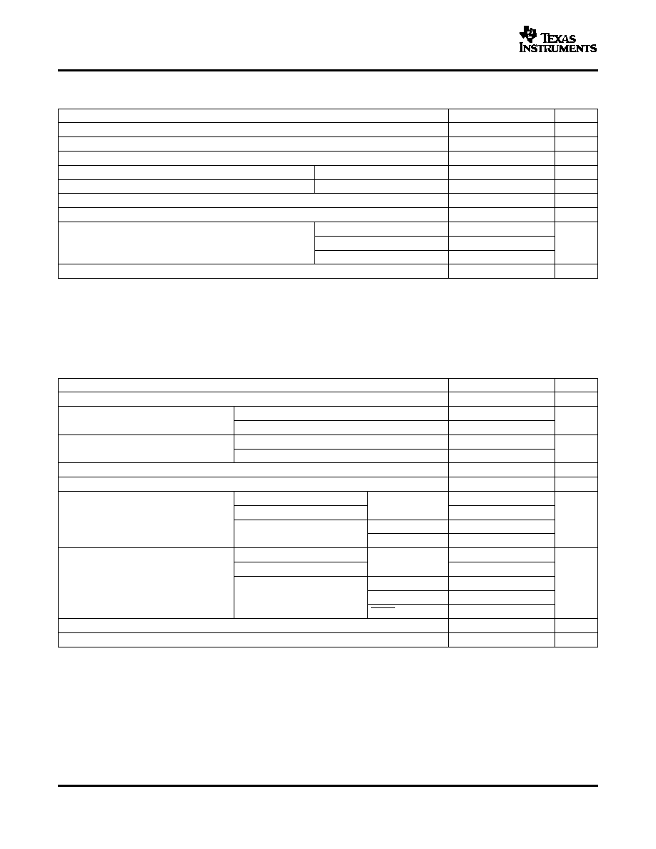
ABSOLUTE MAXIMUM RATINGS
(1)
RECOMMENDED OPERATING CONDITIONS
(1)
SN74ALVCH16903
3.3-V 12-BIT UNIVERSAL BUS DRIVER
WITH PARITY CHECKER AND DUAL 3-STATE OUTPUTS
SCES095D – MARCH 1997 – REVISED SEPTEMBER 2004
over operating free-air temperature range (unless otherwise noted)
MIN
MAX
UNIT
VCC
Supply voltage range
-0.5
4.6
V
VI
Input voltage range(2)
-0.5
4.6
V
VO
Output voltage range(2)(3)
-0.5
VCC + 0.5
V
IIK
Input clamp current
VI < 0
-50
mA
IOK
Output clamp current
VO < 0
-50
mA
IO
Continuous output current
±50
mA
Continuous current through each VCC or GND
±100
mA
DGG package
81
θ
JA
Package thermal impedance(4)
DGV package
86
°C/W
DL package
74
Tstg
Storage temperature range
-65
150
°C
(1)
Stresses beyond those listed under "absolute maximum ratings" may cause permanent damage to the device. These are stress ratings
only, and functional operation of the device at these or any other conditions beyond those indicated under "recommended operating
conditions" is not implied. Exposure to absolute-maximum-rated conditions for extended periods may affect device reliability.
(2)
The input negative-voltage and output voltage ratings may be exceeded if the input and output current ratings are observed.
(3)
This value is limited to 4.6 V maximum.
(4)
The package thermal impedance is calculated in accordance with JESD 51.
MIN
MAX
UNIT
VCC
Supply voltage
2.3
3.6
V
VCC = 2.3 V to 2.7 V
1.7
VIH
High-level input voltage
V
VCC = 2.7 V to 3.6 V
2
VCC = 2.3 V to 2.7 V
0.7
VIL
Low-level input voltage
V
VCC = 2.7 V to 3.6 V
0.8
VI
Input voltage
0
VCC
V
VO
Output voltage
0
VCC
V
VCC = 2.3 V
-12
Y port
VCC = 2.7 V
-12
IOH
High-level output current
mA
PARI/O
-12
VCC = 3 V
Y port
-24
VCC = 2.3 V
12
Y port
VCC = 2.7 V
12
IOL
Low-level output current
PARI/O
12
mA
VCC = 3 V
Y port
24
YERR output
24
t/v
Input transition rise or fall rate
0
10
ns/V
TA
Operating free-air temperature
0
70
°C
(1)
All unused control inputs of the device must be held at VCC or GND to ensure proper device operation. Refer to the TI application report,
Implications of Slow or Floating CMOS Inputs, literature number SCBA004.
4
相关PDF资料 |
PDF描述 |
|---|---|
| SN74ALVCH16973DLR | ALVC/VCX/A SERIES, 8-BIT TRANSCEIVER, TRUE OUTPUT, PDSO48 |
| SN74ALVCH244DWG4 | ALVC/VCX/A SERIES, DUAL 4-BIT DRIVER, TRUE OUTPUT, PDSO20 |
| SN74ALVCH244PWE4 | ALVC/VCX/A SERIES, DUAL 4-BIT DRIVER, TRUE OUTPUT, PDSO20 |
| SN74ALVCH244PWLE | ALVC/VCX/A SERIES, DUAL 4-BIT DRIVER, TRUE OUTPUT, PDSO20 |
| SN74ALVCH244DWR | ALVC/VCX/A SERIES, DUAL 4-BIT DRIVER, TRUE OUTPUT, PDSO20 |
相关代理商/技术参数 |
参数描述 |
|---|---|
| SN74ALVCH16952DGG | 制造商:Rochester Electronics LLC 功能描述: 制造商:Texas Instruments 功能描述: |
| SN74ALVCH16952DGGR | 功能描述:总线收发器 16bit Reg RoHS:否 制造商:Fairchild Semiconductor 逻辑类型:CMOS 逻辑系列:74VCX 每芯片的通道数量:16 输入电平:CMOS 输出电平:CMOS 输出类型:3-State 高电平输出电流:- 24 mA 低电平输出电流:24 mA 传播延迟时间:6.2 ns 电源电压-最大:2.7 V, 3.6 V 电源电压-最小:1.65 V, 2.3 V 最大工作温度:+ 85 C 封装 / 箱体:TSSOP-48 封装:Reel |
| SN74ALVCH16952DGVR | 功能描述:总线收发器 16bit Reg RoHS:否 制造商:Fairchild Semiconductor 逻辑类型:CMOS 逻辑系列:74VCX 每芯片的通道数量:16 输入电平:CMOS 输出电平:CMOS 输出类型:3-State 高电平输出电流:- 24 mA 低电平输出电流:24 mA 传播延迟时间:6.2 ns 电源电压-最大:2.7 V, 3.6 V 电源电压-最小:1.65 V, 2.3 V 最大工作温度:+ 85 C 封装 / 箱体:TSSOP-48 封装:Reel |
| SN74ALVCH16952DL | 功能描述:总线收发器 16bit Reg RoHS:否 制造商:Fairchild Semiconductor 逻辑类型:CMOS 逻辑系列:74VCX 每芯片的通道数量:16 输入电平:CMOS 输出电平:CMOS 输出类型:3-State 高电平输出电流:- 24 mA 低电平输出电流:24 mA 传播延迟时间:6.2 ns 电源电压-最大:2.7 V, 3.6 V 电源电压-最小:1.65 V, 2.3 V 最大工作温度:+ 85 C 封装 / 箱体:TSSOP-48 封装:Reel |
| SN74ALVCH16952DLR | 功能描述:总线收发器 16bit Reg RoHS:否 制造商:Fairchild Semiconductor 逻辑类型:CMOS 逻辑系列:74VCX 每芯片的通道数量:16 输入电平:CMOS 输出电平:CMOS 输出类型:3-State 高电平输出电流:- 24 mA 低电平输出电流:24 mA 传播延迟时间:6.2 ns 电源电压-最大:2.7 V, 3.6 V 电源电压-最小:1.65 V, 2.3 V 最大工作温度:+ 85 C 封装 / 箱体:TSSOP-48 封装:Reel |
发布紧急采购,3分钟左右您将得到回复。