- 您现在的位置:买卖IC网 > PDF目录98102 > SN74ALVCH16903DLR (TEXAS INSTRUMENTS INC) ALVC/VCX/A SERIES, 12-BIT DRIVER, TRUE OUTPUT, PDSO56 PDF资料下载
参数资料
| 型号: | SN74ALVCH16903DLR |
| 厂商: | TEXAS INSTRUMENTS INC |
| 元件分类: | 总线收发器 |
| 英文描述: | ALVC/VCX/A SERIES, 12-BIT DRIVER, TRUE OUTPUT, PDSO56 |
| 封装: | 0.300 INCH, GREEN, PLASTIC, SSOP-56 |
| 文件页数: | 15/18页 |
| 文件大小: | 401K |
| 代理商: | SN74ALVCH16903DLR |
www.ti.com
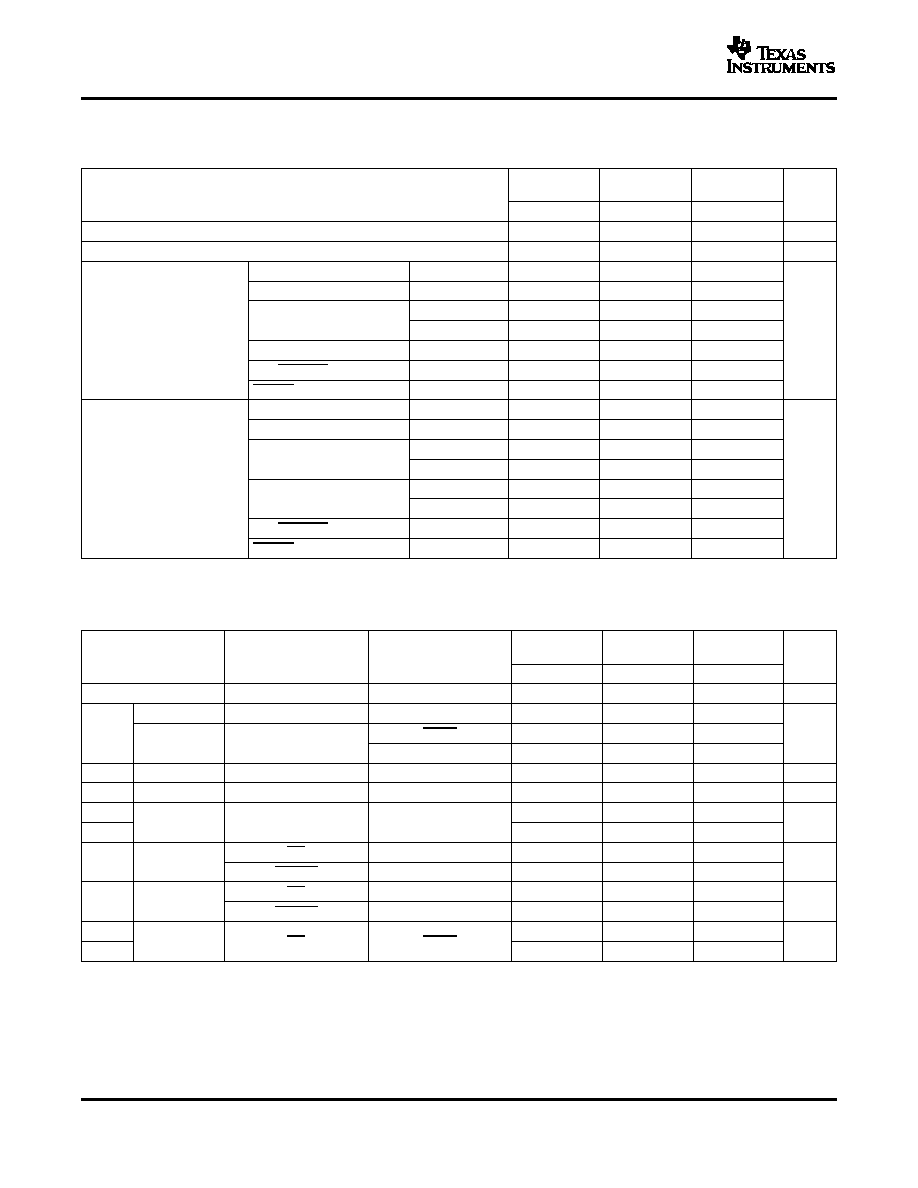
TIMING REQUIREMENTS
SWITCHING CHARACTERISTICS
SN74ALVCH16903
3.3-V 12-BIT UNIVERSAL BUS DRIVER
WITH PARITY CHECKER AND DUAL 3-STATE OUTPUTS
SCES095D – MARCH 1997 – REVISED SEPTEMBER 2004
over recommended ranges of supply voltage and operating free-air temperature (unless otherwise noted) (see Figure 1 and
Figure 4)
VCC = 2.5 V
VCC = 3.3 V
VCC = 2.7 V
± 0.2 V
± 0.3 V
UNIT
MIN
MAX
MIN
MAX
MIN
MAX
fclock
Clock frequency
125
MHz
tw
Pulse duration, CLK
↑
3
ns
1A–12A before CLK
↑
Register mode
1.7
1.9
1.45
1A–10A before CLK
↑
Buffer mode
5.9
5.2
4.4
Register mode
1.2
1.5
1.3
APAR before CLK
↑
tsu
Setup time
Buffer mode
4.6
3.6
3.1
ns
PARI/O before CLK
↑
Both modes
2.4
2
1.7
11A/YERREN before CLK
↑ Buffer mode
2
1.9
1.6
CLKEN before CLK
↑
Register mode
2.5
2.6
2.2
1A–12A after CLK
↑
Register mode
0.4
0.25
0.55
1A–10A after CLK
↑
Buffer mode
0.25
Register mode
0.7
0.4
0.7
APAR after CLK
↑
Buffer mode
0.25
th
Hold time
ns
Register mode
0.25
0.4
PARI/O after CLK
↑
Buffer mode
0.25
0.5
11A/YERREN after CLK
↑
Buffer mode
0.25
0.4
CLKEN after CLK
↑
Register mode
0.25
0.5
0.4
over recommended operating free-air temperature range (unless otherwise noted) (see Figure 1 and Figure 4)
VCC = 2.5 V
VCC = 3.3 V
VCC = 2.7 V
FROM
TO
± 0.2 V
± 0.3 V
PARAMETER
UNIT
(INPUT)
(OUTPUT)
MIN
MAX
MIN
MAX
MIN
MAX
fmax
125
MHz
Buffer mode
A
Y
1
4.4
4.2
1.1
3.8
tpd
YERR
1
5.7
4.9
1.4
4.4
ns
Both modes
CLK
PARI/O
1.2
8.6
7.9
1.7
6.6
tpd(1)
Both modes
CLK
PARI/O
1
6.8
5.2
1.3
4.5
ns
tpd
Both modes
MODE
Y
1
5.9
5.8
1.3
4.9
ns
tPLH
1
6.1
5.5
1.2
4.8
Register mode
CLK
Y
ns
tPHL
1
5.9
4.9
1.2
4.6
OE
Y
1.1
6.5
6.4
1.4
5.4
ten
Both modes
ns
PAROE
PARI/O
1
5.6
6
1
4.8
OE
Y
1
6.4
5.2
1.7
5
tdis
Both modes
ns
PAROE
PARI/O
1
3.2
3.8
1.2
3.8
tPLH
1
3.6
4.2
1.9
4
Both modes
OE
YERR
ns
tPHL
1.2
5.1
4.9
1.5
4.2
(1)
6
相关PDF资料 |
PDF描述 |
|---|---|
| SN74ALVCH16973DLR | ALVC/VCX/A SERIES, 8-BIT TRANSCEIVER, TRUE OUTPUT, PDSO48 |
| SN74ALVCH244DWG4 | ALVC/VCX/A SERIES, DUAL 4-BIT DRIVER, TRUE OUTPUT, PDSO20 |
| SN74ALVCH244PWE4 | ALVC/VCX/A SERIES, DUAL 4-BIT DRIVER, TRUE OUTPUT, PDSO20 |
| SN74ALVCH244PWLE | ALVC/VCX/A SERIES, DUAL 4-BIT DRIVER, TRUE OUTPUT, PDSO20 |
| SN74ALVCH244DWR | ALVC/VCX/A SERIES, DUAL 4-BIT DRIVER, TRUE OUTPUT, PDSO20 |
相关代理商/技术参数 |
参数描述 |
|---|---|
| SN74ALVCH16952DGG | 制造商:Rochester Electronics LLC 功能描述: 制造商:Texas Instruments 功能描述: |
| SN74ALVCH16952DGGR | 功能描述:总线收发器 16bit Reg RoHS:否 制造商:Fairchild Semiconductor 逻辑类型:CMOS 逻辑系列:74VCX 每芯片的通道数量:16 输入电平:CMOS 输出电平:CMOS 输出类型:3-State 高电平输出电流:- 24 mA 低电平输出电流:24 mA 传播延迟时间:6.2 ns 电源电压-最大:2.7 V, 3.6 V 电源电压-最小:1.65 V, 2.3 V 最大工作温度:+ 85 C 封装 / 箱体:TSSOP-48 封装:Reel |
| SN74ALVCH16952DGVR | 功能描述:总线收发器 16bit Reg RoHS:否 制造商:Fairchild Semiconductor 逻辑类型:CMOS 逻辑系列:74VCX 每芯片的通道数量:16 输入电平:CMOS 输出电平:CMOS 输出类型:3-State 高电平输出电流:- 24 mA 低电平输出电流:24 mA 传播延迟时间:6.2 ns 电源电压-最大:2.7 V, 3.6 V 电源电压-最小:1.65 V, 2.3 V 最大工作温度:+ 85 C 封装 / 箱体:TSSOP-48 封装:Reel |
| SN74ALVCH16952DL | 功能描述:总线收发器 16bit Reg RoHS:否 制造商:Fairchild Semiconductor 逻辑类型:CMOS 逻辑系列:74VCX 每芯片的通道数量:16 输入电平:CMOS 输出电平:CMOS 输出类型:3-State 高电平输出电流:- 24 mA 低电平输出电流:24 mA 传播延迟时间:6.2 ns 电源电压-最大:2.7 V, 3.6 V 电源电压-最小:1.65 V, 2.3 V 最大工作温度:+ 85 C 封装 / 箱体:TSSOP-48 封装:Reel |
| SN74ALVCH16952DLR | 功能描述:总线收发器 16bit Reg RoHS:否 制造商:Fairchild Semiconductor 逻辑类型:CMOS 逻辑系列:74VCX 每芯片的通道数量:16 输入电平:CMOS 输出电平:CMOS 输出类型:3-State 高电平输出电流:- 24 mA 低电平输出电流:24 mA 传播延迟时间:6.2 ns 电源电压-最大:2.7 V, 3.6 V 电源电压-最小:1.65 V, 2.3 V 最大工作温度:+ 85 C 封装 / 箱体:TSSOP-48 封装:Reel |
发布紧急采购,3分钟左右您将得到回复。