- 您现在的位置:买卖IC网 > PDF目录98112 > SN74GTL16612ADLR (TEXAS INSTRUMENTS INC) GTL/TVC SERIES, 18-BIT REGISTERED TRANSCEIVER, TRUE OUTPUT, PDSO56 PDF资料下载
参数资料
| 型号: | SN74GTL16612ADLR |
| 厂商: | TEXAS INSTRUMENTS INC |
| 元件分类: | 总线收发器 |
| 英文描述: | GTL/TVC SERIES, 18-BIT REGISTERED TRANSCEIVER, TRUE OUTPUT, PDSO56 |
| 封装: | PLASTIC, SSOP-56 |
| 文件页数: | 7/14页 |
| 文件大小: | 234K |
| 代理商: | SN74GTL16612ADLR |
www.ti.com
DESCRIPTION (CONTINUED)
SN54GTL16612A, SN74GTL16612A
18-BIT LVTTL-TO-GTL+ UNIVERSAL BUS TRANSCEIVERS
SCES187D – JANUARY 1999 – REVISED JULY 2005
Additional design considerations can be found in Application Information at the end of this data sheet.
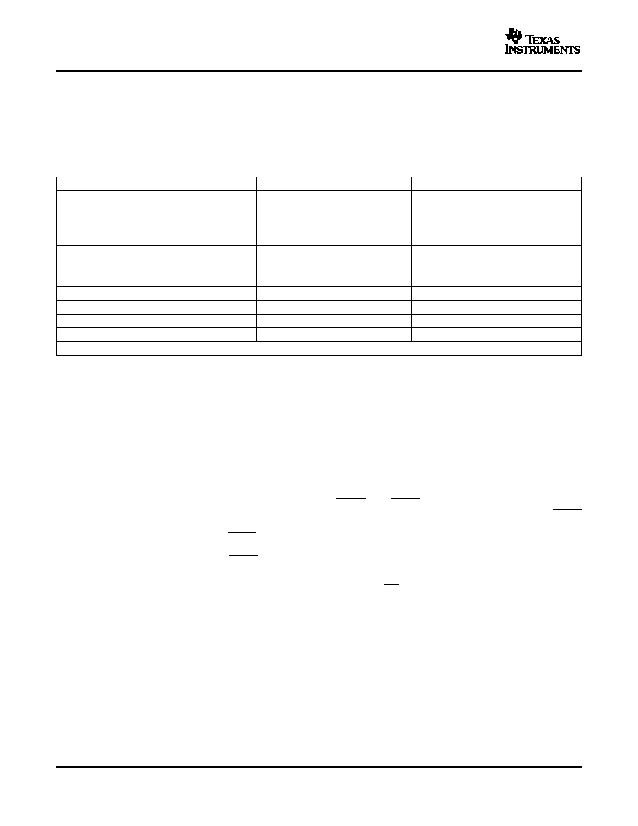
These 18-bit universal bus transceivers combine D-type latches and D-type flip-flops to allow data flow in
transparent, latched, clocked, and clock-enabled modes. These UBTs can replace any of the functions shown in
Table 1.
Table 1. 'GTL16612A UBT Replacement Functions
FUNCTION
8 BIT
9 BIT
10 BIT
16 BIT
18 BIT
Transceiver
'245, '623, '645
'863
'861
'16245, '16623
'16863
Buffer/driver
'241, '244, '541
'827
'16241, '16244, '16541
'16825
Latched transceiver
'543
'16543
'16472
Latch
'373, '573
'843
'841
'16373
'16843
Registered transceiver
'646, '652
'16646, '16652
'16474
Flip-flop
'374, '574
'821
'16374
Standard UBT
'16500, '16501
Universal bus driver
'16835
Registered transceiver with CLK enable
'2952
'16470, '16952
Flip-flop with CLK enable
'377
'823
'16823
Standard UBT with CLK enable
'16600, '16601
'GTL16612A UBT replaces all above functions
xxx
GTL+ is the Texas Instruments (TI) derivative of the Gunning transceiver logic (GTL) JEDEC standard
JESD 8-3. The AC specification of the 'GTL16612A is given only at the preferred higher noise margin GTL+, but
this device can be used at either GTL (V
TT = 1.2 V and VREF = 0.8 V) or GTL+ (VTT = 1.5 V and VREF = 1 V)
signal levels.
The B port normally operates at GTL or GTL+ levels, while the A-port and control inputs are compatible with
LVTTL logic levels and are 5-V tolerant. V
REF is the reference input voltage for the B port.
To improve signal integrity, the 'GTL16612A B-port output transition time is optimized for distributed backplane
loads.
V
CC (5 V) supplies the internal and GTL circuitry, while VCC (3.3 V) supplies the LVTTL output buffers.
Data flow in each direction is controlled by output-enable (OEAB and OEBA), latch-enable (LEAB and LEBA),
and clock (CLKAB and CLKBA) inputs. The clock or latch enable can be controlled by the clock-enable (CEAB
and CEBA) inputs. For A-to-B data flow, the devices operate in the transparent mode when LEAB is high. When
LEAB is low, the A data is latched if CEAB is low and CLKAB is held at a high or low logic level. If LEAB is low,
the A data is stored in the latch/flip-flop on the low-to-high transition of CLKAB if CEAB also is low. When OEAB
is low, the outputs are active. When OEAB is high, the outputs are in the high-impedance state. Data flow for B
to A is similar to that for A to B, but uses OEBA, LEBA, CLKBA, and CEBA.
To ensure the high-impedance state during power up or power down, OE should be tied to V
CC through a pullup
resistor; the minimum value of the resistor is determined by the current-sinking capability of the driver.
Active bus-hold circuitry holds unused or undriven LVTTL inputs at a valid logic state. Use of pullup or pulldown
resistors with the bus-hold circuitry is not recommended.
These devices are fully specified for partial-power-down applications using I
off. The Ioff circuitry disables the
outputs, preventing damaging current backflow through the devices when they are powered down.
The SN54GTL16612A is characterized for operation over the full military temperature range of –55°C to 125°C.
The SN74GTL16612A is characterized for operation from –40°C to 85°C.
2
相关PDF资料 |
PDF描述 |
|---|---|
| SN74GTL16612DGGR | GTL/TVC SERIES, 18-BIT REGISTERED TRANSCEIVER, TRUE OUTPUT, PDSO56 |
| SN74GTLP1394DR | GTLP SERIES, 2-BIT TRANSCEIVER, CONFIGURABLE OUTPUT, PDSO16 |
| SN74GTLP1394DGVR | GTLP SERIES, 2-BIT TRANSCEIVER, CONFIGURABLE OUTPUT, PDSO16 |
| SN74GTLP2033DGVR | GTLP SERIES, 8-BIT REGISTERED TRANSCEIVER, INVERTED OUTPUT, PDSO48 |
| SN74GTLP2034DGVR | GTLP SERIES, 8-BIT REGISTERED TRANSCEIVER, TRUE OUTPUT, PDSO48 |
相关代理商/技术参数 |
参数描述 |
|---|---|
| SN74GTL16612DGGR | 功能描述:转换 - 电压电平 18Bit LVTTL/GTL/GTL+ Univ Bus Xcvr RoHS:否 制造商:Micrel 类型:CML/LVDS/LVPECL to LVCMOS/LVTTL 传播延迟时间:1.9 ns 电源电流:14 mA 电源电压-最大:3.6 V 电源电压-最小:3 V 最大工作温度:+ 85 C 安装风格:SMD/SMT 封装 / 箱体:MLF-8 |
| SN74GTL16612DL | 功能描述:转换 - 电压电平 18Bit LVTTL/GTL/GTL+ Univ Bus Xcvr RoHS:否 制造商:Micrel 类型:CML/LVDS/LVPECL to LVCMOS/LVTTL 传播延迟时间:1.9 ns 电源电流:14 mA 电源电压-最大:3.6 V 电源电压-最小:3 V 最大工作温度:+ 85 C 安装风格:SMD/SMT 封装 / 箱体:MLF-8 |
| SN74GTL16612DLG4 | 功能描述:转换 - 电压电平 18Bit LVTTL/GTL/GTL+ Univ Bus Xcvr RoHS:否 制造商:Micrel 类型:CML/LVDS/LVPECL to LVCMOS/LVTTL 传播延迟时间:1.9 ns 电源电流:14 mA 电源电压-最大:3.6 V 电源电压-最小:3 V 最大工作温度:+ 85 C 安装风格:SMD/SMT 封装 / 箱体:MLF-8 |
| SN74GTL16612DLR | 功能描述:转换 - 电压电平 18Bit LVTTL/GTL/GTL+ Univ Bus Xcvr RoHS:否 制造商:Micrel 类型:CML/LVDS/LVPECL to LVCMOS/LVTTL 传播延迟时间:1.9 ns 电源电流:14 mA 电源电压-最大:3.6 V 电源电压-最小:3 V 最大工作温度:+ 85 C 安装风格:SMD/SMT 封装 / 箱体:MLF-8 |
| SN74GTL16612DLRG4 | 功能描述:转换 - 电压电平 3-8-Line Decoder Demltplxr RoHS:否 制造商:Micrel 类型:CML/LVDS/LVPECL to LVCMOS/LVTTL 传播延迟时间:1.9 ns 电源电流:14 mA 电源电压-最大:3.6 V 电源电压-最小:3 V 最大工作温度:+ 85 C 安装风格:SMD/SMT 封装 / 箱体:MLF-8 |
发布紧急采购,3分钟左右您将得到回复。