- 您现在的位置:买卖IC网 > PDF目录98122 > SN74LVC1G07YZAR (TEXAS INSTRUMENTS INC) LVC/LCX/Z SERIES, 1-INPUT NON-INVERT GATE, BGA5 PDF资料下载
参数资料
| 型号: | SN74LVC1G07YZAR |
| 厂商: | TEXAS INSTRUMENTS INC |
| 元件分类: | 门电路 |
| 英文描述: | LVC/LCX/Z SERIES, 1-INPUT NON-INVERT GATE, BGA5 |
| 封装: | GREEN, MO-211EA, DSBGA-5 |
| 文件页数: | 1/22页 |
| 文件大小: | 675K |
| 代理商: | SN74LVC1G07YZAR |
www.ti.com
FEATURES
3
2
4
5
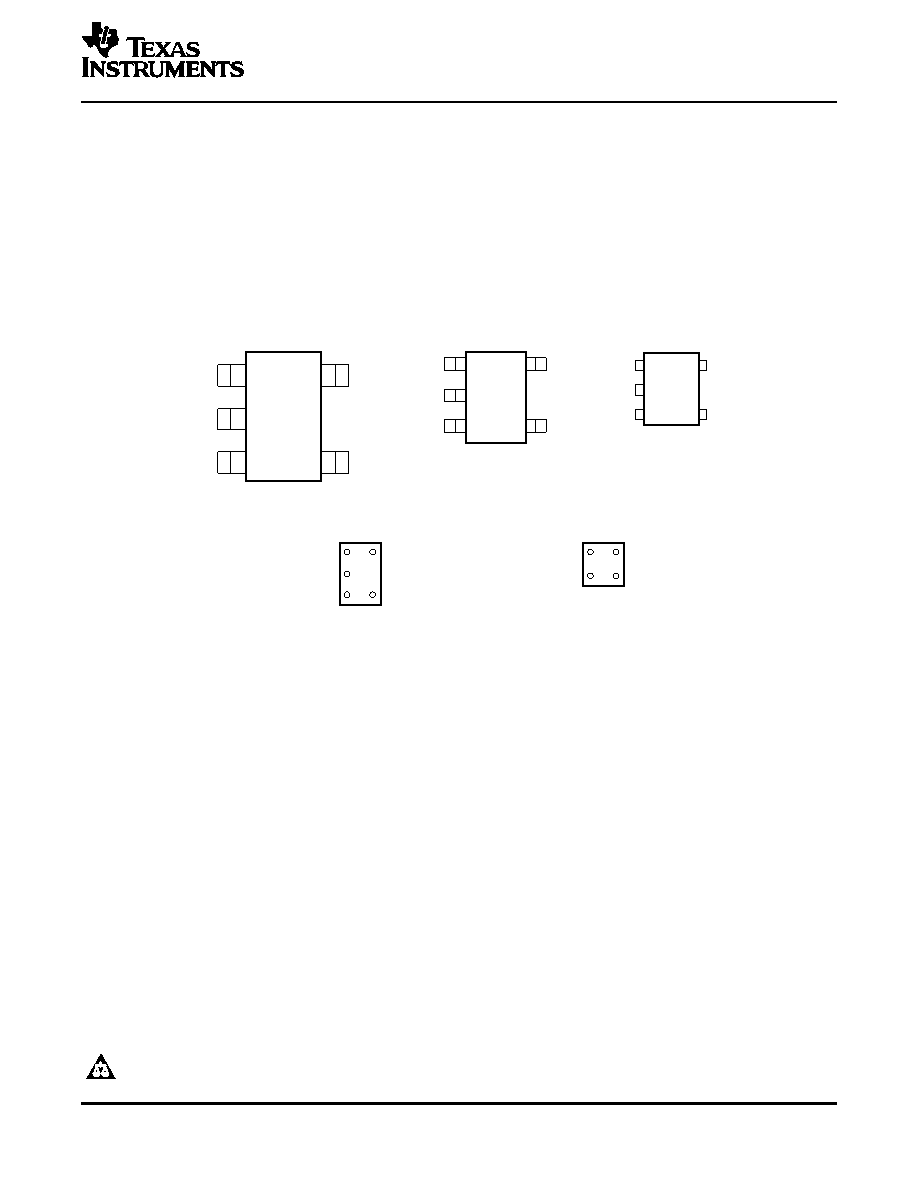
1
NC
VCC
Y
A
GND
DBV PACKAGE
(TOP VIEW)
YEA, YEP, YZA, OR YZP PACKAGE
(BOTTOM VIEW)
DCK PACKAGE
(TOP VIEW)
3
2
4
5
1
NC
VCC
Y
A
GND
3
2
4
5
1
NC
Y
A
GND
DNU
GND
VCC
Y
A
DRL PACKAGE
(TOP VIEW)
See mechanical drawings for dimensions.
1
4
2
3
5
VCC
DNU Do not use
YZV PACKAGE
(BOTTOM VIEW)
GND
VCC
Y
A
3
1
2
4
DESCRIPTION/ORDERING INFORMATION
SN74LVC1G07
SINGLE BUFFER/DRIVER
WITH OPEN-DRAIN OUTPUT
SCES296T – FEBRUARY 2000 – REVISED OCTOBER 2005
Available in the Texas Instruments
Ioff Supports Partial-Power-Down Mode
NanoStar and NanoFree Packages
Operation
Supports 5-V V
CC Operation
Latch-Up Performance Exceeds 100 mA Per
JESD 78, Class II
Input and Open-Drain Output Accept
Voltages up to 5.5 V
ESD Protection Exceeds JESD 22
Max t
pd of 4.2 ns at 3.3 V
– 2000-V Human-Body Model (A114-A)
Low Power Consumption, 10-
A Max I
CC
– 200-V Machine Model (A115-A)
±24-mA Output Drive at 3.3 V
– 1000-V Charged-Device Model (C101)
This single buffer/driver is designed for 1.65-V to 5.5-V VCC operation.
NanoStar and NanoFree package technology is a major breakthrough in IC packaging concepts, using the
die as the package.
The output of the SN74LVC1G07 device is open drain and can be connected to other open-drain outputs to
implement active-low wired-OR or active-high wired-AND functions. The maximum sink current is 32 mA.
This device is fully specified for partial-power-down applications using Ioff.The Ioff circuitry disables the outputs,
preventing damaging current backflow through the device when it is powered down.
Please be aware that an important notice concerning availability, standard warranty, and use in critical applications of Texas
Instruments semiconductor products and disclaimers thereto appears at the end of this data sheet.
NanoStar, NanoFree are trademarks of Texas Instruments.
PRODUCTION DATA information is current as of publication date.
Copyright 2000–2005, Texas Instruments Incorporated
Products conform to specifications per the terms of the Texas
Instruments standard warranty. Production processing does not
necessarily include testing of all parameters.
相关PDF资料 |
PDF描述 |
|---|---|
| SN74LVC1G08DBVR | LVC/LCX/Z SERIES, 2-INPUT AND GATE, PDSO5 |
| SN74LVC1G08DRLRG4 | LVC/LCX/Z SERIES, 2-INPUT AND GATE, PDSO5 |
| SN74LVC1G08DRLR | LVC/LCX/Z SERIES, 2-INPUT AND GATE, PDSO5 |
| SN74LVC1G08YEPR | LVC/LCX/Z SERIES, 2-INPUT AND GATE, PBGA5 |
| SN74LVC1G10DCKR | LVC/LCX/Z SERIES, 3-INPUT NAND GATE, PDSO6 |
相关代理商/技术参数 |
参数描述 |
|---|---|
| SN74LVC1G07YZPR | 功能描述:缓冲器和线路驱动器 SNGL Buffer/Driver RoHS:否 制造商:Micrel 输入线路数量:1 输出线路数量:2 极性:Non-Inverting 电源电压-最大:+/- 5.5 V 电源电压-最小:+/- 2.37 V 最大工作温度:+ 85 C 安装风格:SMD/SMT 封装 / 箱体:MSOP-8 封装:Reel |
| SN74LVC1G07YZTR | 制造商:Texas Instruments 功能描述: |
| SN74LVC1G07YZVR | 功能描述:缓冲器和线路驱动器 Single Buffer/Driver RoHS:否 制造商:Micrel 输入线路数量:1 输出线路数量:2 极性:Non-Inverting 电源电压-最大:+/- 5.5 V 电源电压-最小:+/- 2.37 V 最大工作温度:+ 85 C 安装风格:SMD/SMT 封装 / 箱体:MSOP-8 封装:Reel |
| SN74LVC1G0832DBVR | 功能描述:逻辑门 Sngl 3 Inpt Pos ANDOR Gate RoHS:否 制造商:Texas Instruments 产品:OR 逻辑系列:LVC 栅极数量:2 线路数量(输入/输出):2 / 1 高电平输出电流:- 16 mA 低电平输出电流:16 mA 传播延迟时间:3.8 ns 电源电压-最大:5.5 V 电源电压-最小:1.65 V 最大工作温度:+ 125 C 安装风格:SMD/SMT 封装 / 箱体:DCU-8 封装:Reel |
| SN74LVC1G0832DBVT | 功能描述:逻辑门 SNGL 3 Input Pos AND OR Gate RoHS:否 制造商:Texas Instruments 产品:OR 逻辑系列:LVC 栅极数量:2 线路数量(输入/输出):2 / 1 高电平输出电流:- 16 mA 低电平输出电流:16 mA 传播延迟时间:3.8 ns 电源电压-最大:5.5 V 电源电压-最小:1.65 V 最大工作温度:+ 125 C 安装风格:SMD/SMT 封装 / 箱体:DCU-8 封装:Reel |
发布紧急采购,3分钟左右您将得到回复。