- 您现在的位置:买卖IC网 > PDF目录98141 > SPAK56F802TA60 (MOTOROLA INC) 0-BIT, 60 MHz, OTHER DSP, PQFP32 PDF资料下载
参数资料
| 型号: | SPAK56F802TA60 |
| 厂商: | MOTOROLA INC |
| 元件分类: | 数字信号处理 |
| 英文描述: | 0-BIT, 60 MHz, OTHER DSP, PQFP32 |
| 封装: | 7 X 7 MM, 0.80 MM PITCH, 1.40 MM HEIGHT, PLASTIC, LQFP-32 |
| 文件页数: | 3/39页 |
| 文件大小: | 573K |
| 代理商: | SPAK56F802TA60 |
第1页第2页当前第3页第4页第5页第6页第7页第8页第9页第10页第11页第12页第13页第14页第15页第16页第17页第18页第19页第20页第21页第22页第23页第24页第25页第26页第27页第28页第29页第30页第31页第32页第33页第34页第35页第36页第37页第38页第39页
General Characteristics
MOTOROLA
56F802 Technical Data
11
Part 3 Specifications
3.1 General Characteristics
The 56F802 is fabricated in high-density CMOS with 5-volt tolerant TTL-compatible digital inputs. The
term “5-volt tolerant” refers to the capability of an I/O pin, built on a 3.3V compatible process technology,
to withstand a voltage up to 5.5V without damaging the device. Many systems have a mixture of devices
designed for 3.3V and 5V power supplies. In such systems, a bus may carry both 3.3V and 5V- compatible
I/O voltage levels (a standard 3.3V I/O is designed to receive a maximum voltage of 3.3V
± 10% during
normal operation without causing damage). This 5V-tolerant capability therefore offers the power savings
of 3.3V I/O levels while being able to receive 5V levels without being damaged.
Absolute maximum ratings given in Table 12 are stress ratings only, and functional operation at the
maximum is not guaranteed. Stress beyond these ratings may affect device reliability or cause permanent
damage to the device.
The 56F802 DC and AC electrical specifications are preliminary and are from design simulations. These
specifications may not be fully tested or guaranteed at this early stage of the product life cycle. Finalized
specifications will be published after complete characterization and device qualifications have been
completed.
CAUTION
This device contains protective circuitry to guard against
damage due to high static voltage or electrical fields.
However,
normal
precautions
are
advised
to
avoid
application of any voltages higher than maximum rated
voltages
to
this
high-impedance
circuit.
Reliability
of
operation is enhanced if unused inputs are tied to an
appropriate voltage level.
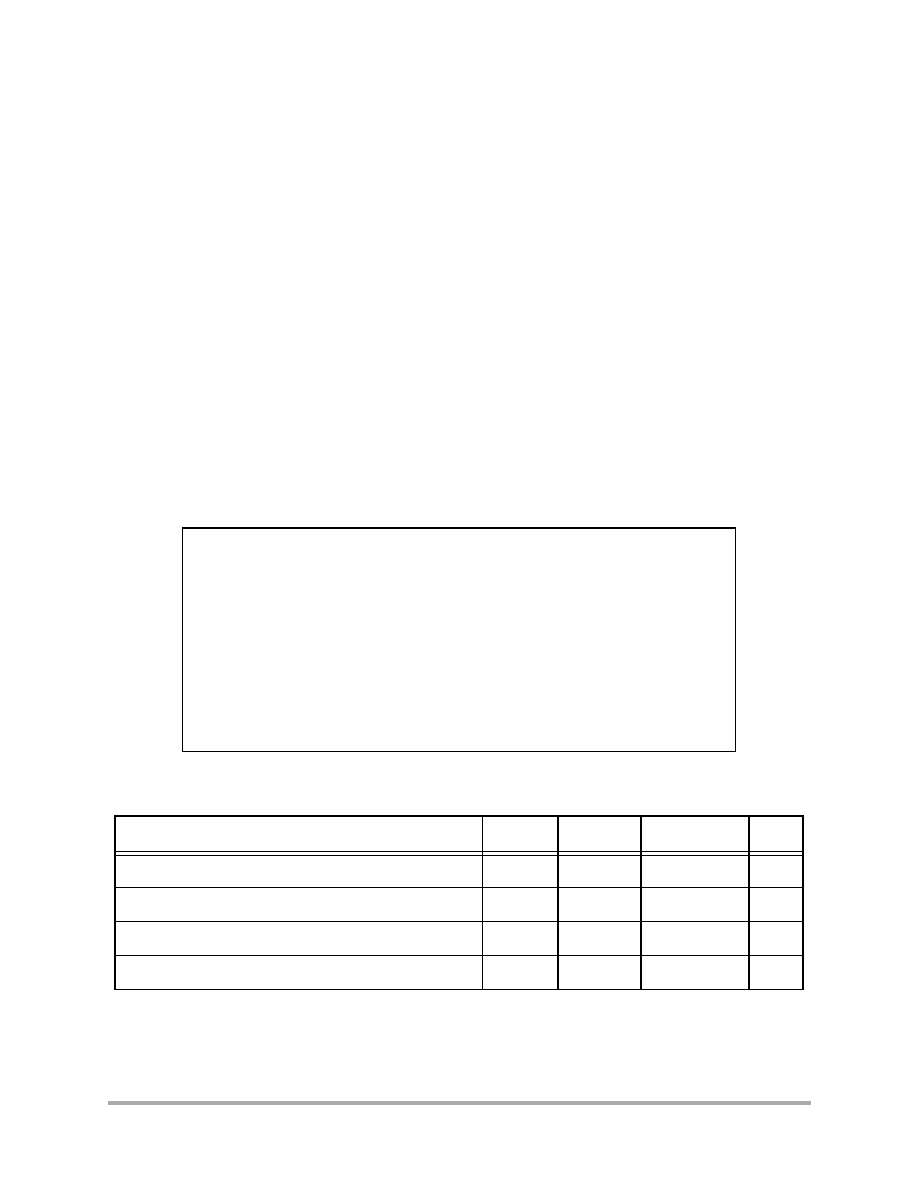
Table 12. Absolute Maximum Ratings
Characteristic
Symbol
Min
Max
Unit
Supply voltage
VDD
VSS – 0.3
VSS + 4.0
V
All other input voltages, excluding Analog inputs
VIN
VSS – 0.3
VSS + 5.5V
V
Analog Inputs ANAx, VREF
VIN
VSS – 0.3
VDDA + 0.3V
V
Current drain per pin excluding VDD, VSS, & PWM ouputs
I
—
10
mA
相关PDF资料 |
PDF描述 |
|---|---|
| SPAK56F805FV80 | 16-BIT, 8 MHz, OTHER DSP, PQFP144 |
| SPAK56F807VF80 | 16-BIT, 80 MHz, OTHER DSP, PBGA160 |
| SPAK56F807VF80 | 16-BIT, 80 MHz, OTHER DSP, PBGA160 |
| SPAK56F826BU80 | 16-BIT, 80 MHz, OTHER DSP, PQFP100 |
| SPAK56F8346FV60 | 16-BIT, 240 MHz, OTHER DSP, PQFP144 |
相关代理商/技术参数 |
参数描述 |
|---|---|
| SPAK56F803BU80 | 制造商:Freescale Semiconductor 功能描述: |
| SPAK56F805FV80 | 制造商:Freescale Semiconductor 功能描述: |
| SPAKDSP303AG100 | 功能描述:数字信号处理器和控制器 - DSP, DSC SPAKDSP303AG100 RoHS:否 制造商:Microchip Technology 核心:dsPIC 数据总线宽度:16 bit 程序存储器大小:16 KB 数据 RAM 大小:2 KB 最大时钟频率:40 MHz 可编程输入/输出端数量:35 定时器数量:3 设备每秒兆指令数:50 MIPs 工作电源电压:3.3 V 最大工作温度:+ 85 C 封装 / 箱体:TQFP-44 安装风格:SMD/SMT |
| SPAKDSP303GC100 | 制造商:Motorola Inc 功能描述: |
| SPAKDSP303VF100 | 功能描述:IC DSP 24BIT 100MHZ 196-MAPBGA RoHS:否 类别:集成电路 (IC) >> 嵌入式 - DSP(数字式信号处理器) 系列:DSP563xx 标准包装:40 系列:TMS320DM64x, DaVinci™ 类型:定点 接口:I²C,McASP,McBSP 时钟速率:400MHz 非易失内存:外部 芯片上RAM:160kB 电压 - 输入/输出:3.30V 电压 - 核心:1.20V 工作温度:0°C ~ 90°C 安装类型:表面贴装 封装/外壳:548-BBGA,FCBGA 供应商设备封装:548-FCBGA(27x27) 包装:托盘 配用:TMDSDMK642-0E-ND - DEVELPER KIT W/NTSC CAMERA296-23038-ND - DSP STARTER KIT FOR TMS320C6416296-23059-ND - FLASHBURN PORTING KIT296-23058-ND - EVAL MODULE FOR DM642TMDSDMK642-ND - DEVELOPER KIT W/NTSC CAMERA |
发布紧急采购,3分钟左右您将得到回复。