- 您现在的位置:买卖IC网 > PDF目录98141 > SPAK56F802TA60 (MOTOROLA INC) 0-BIT, 60 MHz, OTHER DSP, PQFP32 PDF资料下载
参数资料
| 型号: | SPAK56F802TA60 |
| 厂商: | MOTOROLA INC |
| 元件分类: | 数字信号处理 |
| 英文描述: | 0-BIT, 60 MHz, OTHER DSP, PQFP32 |
| 封装: | 7 X 7 MM, 0.80 MM PITCH, 1.40 MM HEIGHT, PLASTIC, LQFP-32 |
| 文件页数: | 38/39页 |
| 文件大小: | 573K |
| 代理商: | SPAK56F802TA60 |
第1页第2页第3页第4页第5页第6页第7页第8页第9页第10页第11页第12页第13页第14页第15页第16页第17页第18页第19页第20页第21页第22页第23页第24页第25页第26页第27页第28页第29页第30页第31页第32页第33页第34页第35页第36页第37页当前第38页第39页
8
56F802 Technical Data
MOTOROLA
2.2 Power and Ground Signals
2.3 Interrupt and Program Control Signals
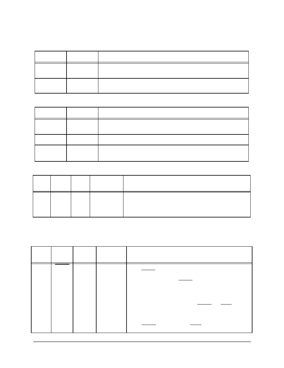
Table 3. Power Inputs
No. of Pins
Signal Name
Signal Description
2
VDD
Power—These pins provide power to the internal structures of the chip, and
should all be attached to VDD.
1
VDDA
Analog Power—This pin is a dedicated power pin for the analog portion of the
chip and should be connected to a low noise 3.3V supply.
Table 4. Grounds
No. of Pins
Signal Name
Signal Description
2
VSS
GND—These pins provide grounding for the internal structures of the chip, and
should all be attached to VSS.
1
VSSA
Analog Ground—This pin supplies an analog ground.
1
TCS
TCS—This Schmitt pin is reserved for factory use and must be tied to VSS for
normal use. In block diagrams, this pin is considered an additional VSS.
Table 5. Supply Capacitors and VPP
No. of
Pins
Signal
Name
Signal
Type
State During
Reset
Signal Description
2
VCAPC
Supply
VCAPC—Connect each pin to a 2.2
F or greater bypass
capacitor in order to bypass the core logic voltage regulator
(required for proper chip operation). For more information, refer to
Table 6. Program Control Signals
No. of
Pins
Signal
Name
Signal
Type
State During
Reset
Signal Description
1
RESET
Input
(Schmitt)
Input
Reset—This input is a direct hardware reset on the processor.
When RESET is asserted low, the hybrid controller is initialized
and placed in the Reset state. A Schmitt trigger input is used for
noise immunity. When the RESET pin is deasserted, the initial
chip operating mode is latched from the EXTBOOT pin. The
internal reset signal will be deasserted synchronous with the
internal clocks, after a fixed number of internal clocks.
To ensure complete hardware reset, RESET and TRST should
be asserted together. The only exception occurs in a debugging
environment when a hardware device reset is required and it is
necessary not to reset the OnCE/JTAG module. In this case,
assert RESET, but do not assert TRST.
相关PDF资料 |
PDF描述 |
|---|---|
| SPAK56F805FV80 | 16-BIT, 8 MHz, OTHER DSP, PQFP144 |
| SPAK56F807VF80 | 16-BIT, 80 MHz, OTHER DSP, PBGA160 |
| SPAK56F807VF80 | 16-BIT, 80 MHz, OTHER DSP, PBGA160 |
| SPAK56F826BU80 | 16-BIT, 80 MHz, OTHER DSP, PQFP100 |
| SPAK56F8346FV60 | 16-BIT, 240 MHz, OTHER DSP, PQFP144 |
相关代理商/技术参数 |
参数描述 |
|---|---|
| SPAK56F803BU80 | 制造商:Freescale Semiconductor 功能描述: |
| SPAK56F805FV80 | 制造商:Freescale Semiconductor 功能描述: |
| SPAKDSP303AG100 | 功能描述:数字信号处理器和控制器 - DSP, DSC SPAKDSP303AG100 RoHS:否 制造商:Microchip Technology 核心:dsPIC 数据总线宽度:16 bit 程序存储器大小:16 KB 数据 RAM 大小:2 KB 最大时钟频率:40 MHz 可编程输入/输出端数量:35 定时器数量:3 设备每秒兆指令数:50 MIPs 工作电源电压:3.3 V 最大工作温度:+ 85 C 封装 / 箱体:TQFP-44 安装风格:SMD/SMT |
| SPAKDSP303GC100 | 制造商:Motorola Inc 功能描述: |
| SPAKDSP303VF100 | 功能描述:IC DSP 24BIT 100MHZ 196-MAPBGA RoHS:否 类别:集成电路 (IC) >> 嵌入式 - DSP(数字式信号处理器) 系列:DSP563xx 标准包装:40 系列:TMS320DM64x, DaVinci™ 类型:定点 接口:I²C,McASP,McBSP 时钟速率:400MHz 非易失内存:外部 芯片上RAM:160kB 电压 - 输入/输出:3.30V 电压 - 核心:1.20V 工作温度:0°C ~ 90°C 安装类型:表面贴装 封装/外壳:548-BBGA,FCBGA 供应商设备封装:548-FCBGA(27x27) 包装:托盘 配用:TMDSDMK642-0E-ND - DEVELPER KIT W/NTSC CAMERA296-23038-ND - DSP STARTER KIT FOR TMS320C6416296-23059-ND - FLASHBURN PORTING KIT296-23058-ND - EVAL MODULE FOR DM642TMDSDMK642-ND - DEVELOPER KIT W/NTSC CAMERA |
发布紧急采购,3分钟左右您将得到回复。